SNVSAD9 April 2016 LM5175-Q1
PRODUCTION DATA.
- 1 Features
- 2 Applications
- 3 Description
- 4 Simplified Schematic
- 5 Revision History
- 6 Pin Configuration and Functions
- 7 Specifications
-
8 Detailed Description
- 8.1 Overview
- 8.2 Functional Block Diagram
- 8.3
Feature Description
- 8.3.1 Fixed Frequency Valley/Peak Current Mode Control with Slope Compensation
- 8.3.2 VCC Regulator and Optional BIAS Input
- 8.3.3 Enable/UVLO
- 8.3.4 Soft-Start
- 8.3.5 Overcurrent Protection
- 8.3.6 Average Input/Output Current Limiting
- 8.3.7 CCM/DCM Operation
- 8.3.8 Frequency and Synchronization (RT/SYNC)
- 8.3.9 Frequency Dithering
- 8.3.10 Output Overvoltage Protection (OVP)
- 8.3.11 Power Good (PGOOD)
- 8.3.12 Gm Error Amplifier
- 8.3.13 Integrated Gate Drivers
- 8.3.14 Thermal Shutdown
- 8.4 Device Functional Modes
-
9 Application and Implementation
- 9.1 Application Information
- 9.2
Typical Application
- 9.2.1 Design Requirements
- 9.2.2
Detailed Design Procedure
- 9.2.2.1 Frequency
- 9.2.2.2 VOUT
- 9.2.2.3 Inductor Selection
- 9.2.2.4 Output Capacitor
- 9.2.2.5 Input Capacitor
- 9.2.2.6 Sense Resistor (RSENSE)
- 9.2.2.7 Slope Compensation
- 9.2.2.8 UVLO
- 9.2.2.9 Soft-Start Capacitor
- 9.2.2.10 Dither Capacitor
- 9.2.2.11 MOSFETs QH1 and QL1
- 9.2.2.12 MOSFETs QH2 and QL2
- 9.2.2.13 Frequency Compensation
- 9.2.3 Application Curves
- 10Power Supply Recommendations
- 11Layout
- 12Device and Documentation Support
- 13Mechanical, Packaging, and Orderable Information
Package Options
Mechanical Data (Package|Pins)
- PWP|28
Thermal pad, mechanical data (Package|Pins)
- PWP|28
Orderable Information
1 Features
- Qualified for Automotive Applications
- AEC-Q100 Qualified with the following results:
- Device Temperature Grade 1: –40°C to +125°C Ambient Operating Temperature Range
- Device HBM ESD Classification Level 2
- Device CDM ESD Classification Level C4B
- Single Inductor Buck-Boost Controller for Step-Up/Step-Down DC/DC Conversion
- Wide VIN Range: 3.5 V to 42 V, 60 V Maximum
- Flexible VOUT Range: 0.8 V to 55 V
- VOUT Short Protection
- High Efficiency Buck-Boost Transition
- Adjustable Switching Frequency
- Optional Frequency Sync and Dithering
- Integrated 2-A MOSFET Gate Drivers
- Cycle-by-Cycle Current Limit and Optional Hiccup
- Optional Input or Output Average Current Limiting
- Programmable Input UVLO and Soft-Start
- Power Good and Output Overvoltage Protection
- Selectable CCM or DCM with Pulse Skipping
- HTSSOP-28 Package
2 Applications
- Automotive Start-Stop Systems
- Backup Battery and Supercapacitor Charging
- Industrial PC Power Supplies
- USB Power Delivery
- LED Lighting
3 Description
The LM5175-Q1 is a synchronous four-switch buck-boost DC/DC controller capable of regulating the output voltage at, above, or below the input voltage. The LM5175-Q1 operates over a wide input voltage range of 3.5 V to 42 V (60 V maximum) to support a variety of applications.
The LM5175-Q1 employs current-mode control both in buck and boost modes of operation for superior load and line regulation. The switching frequency is programmed by an external resistor and can be synchronized to an external clock signal.
The device also features a programmable soft-start function and offers protection features including cycle-by-cycle current limiting, input undervoltage lockout (UVLO), output overvoltage protection (OVP), and thermal shutdown. In addition, the LM5175-Q1 features selectable Continuous Conduction Mode (CCM) or Discontinuous Conduction Mode (DCM) operation, optional average input or output current limiting, optional spread spectrum to reduce peak EMI, and optional hiccup mode protection in sustained overload conditions.
Device Information(1)
| ORDER NUMBER | PACKAGE | BODY SIZE |
|---|---|---|
| LM5175-Q1 | HTSSOP-28 | 9.7 mm x 4.4 mm |
- For all available packages, see the orderable addendum at the end of the data sheet.
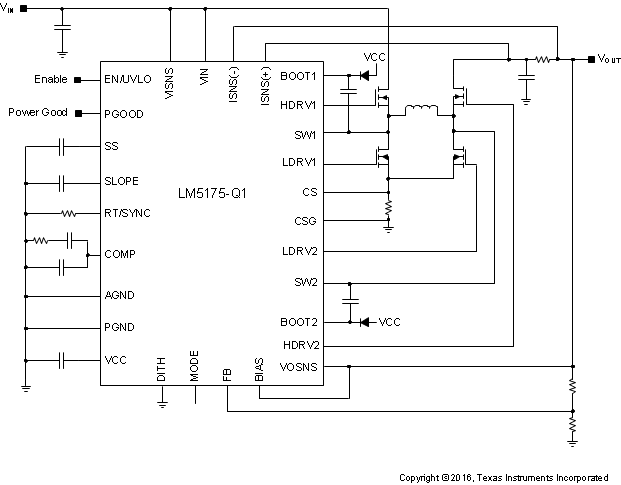
4 Simplified Schematic
