SBOS197F December 2001 – August 2015 OPA657
PRODUCTION DATA.
- 1 Features
- 2 Applications
- 3 Description
- 4 Revision History
- 5 Related Operational Amplifier Products
- 6 Pin Configuration and Functions
- 7 Specifications
- 8 Detailed Description
- 9 Application and Implementation
- 10Power Supply Recommendations
- 11Layout
- 12Device and Documentation Support
- 13Mechanical, Packaging, and Orderable Information
Package Options
Mechanical Data (Package|Pins)
Thermal pad, mechanical data (Package|Pins)
Orderable Information
1 Features
- High Gain Bandwidth Product: 1.6 GHz
- High Bandwidth 275 MHz (G = 10)
- Slew Rate 700 V/µs (G = 10, 1-V Step)
- Available in High Grade With Improved DC Specifications
- Operating Temperature Range: –40°C to 85°C
- Low-Input Offset Voltage: ±250 µV
- Low-Input Bias Current: 2 pA
- Low-Input Voltage Noise: 4.8 nV/√Hz
- High-Output Current: 70 mA
- Fast Overdrive Recovery
2 Applications
- Wideband Photodiode Amplifier
- Wafer Scanning Equipment
- ADC Input Amplifier
- Test and Measurement Front End
- High Gain Precision Amplifier
- Optical Time Domain Reflectometry (OTDR)
3 Description
The OPA657 device combines a high-gain bandwidth, low-distortion, voltage-feedback operational amplifier with a low-voltage noise JFET-input stage to offer a very high dynamic range amplifier for high-precision ADC (analog-to-digital converter) driving or wideband transimpedance applications. Photodiode applications see improved noise and bandwidth using this decompensated, high-gain bandwidth amplifier.
Very low level signals can be significantly amplified in a single OPA657 gain stage with exceptional bandwidth and accuracy. Having a high 1.6-GHz gain bandwidth product gives greater than 10-MHz signal bandwidths up to gains of 160 V/V (44 dB). The very low input bias current and capacitance supports this performance even for relatively high source impedances.
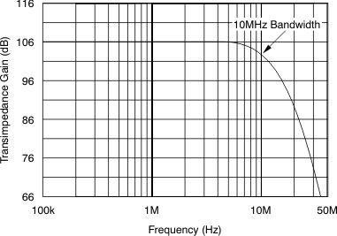
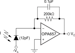
Broadband photodetector applications benefit from the low-voltage noise JFET inputs for the OPA657. The JFET input contributes virtually no current noise while for broadband applications, a low voltage noise is also required. The low 4.8 nV/√Hz input voltage noise provides exceptional input sensitivity for higher bandwidth applications. The example shown below gives a total equivalent input noise current of 1.8 pA/√Hz over a 10-MHz bandwidth.
Device Information(1)
| PART NUMBER | PACKAGE | BODY SIZE (NOM) |
|---|---|---|
| OPA657 | SOT-23 (5) | 2.90 mm × 1.60 mm |
| SOIC (8) | 4.90 mm × 3.91 mm |
- For all available packages, see the orderable addendum at the end of the data sheet.
Frequency Response of 200-kΩ Transimpedance Amplifier

Wideband Photodiode Transimpedance Amplifier
