SCDS175A September 2004 – December 2022 SN74CBT3383C
PRODUCTION DATA
- 1 Features
- 2 Applications
- 3 Description
- 4 Revision History
- 5 Description (continued)
- 6 Pin Configuration and Functions
- 7 Specifications
- 8 Parameter Measurement Information
- 9 Detailed Description
- 10Application and Implementation
- 11Power Supply Recommendations
- 12Layout
- 13Device and Documentation Support
- 14Mechanical, Packaging, and Orderable Information
Package Options
Mechanical Data (Package|Pins)
Thermal pad, mechanical data (Package|Pins)
Orderable Information
1 Features
- Undershoot protection for off-isolation on A and B ports up to −2 V
- Bidirectional data flow, with near-zero propagation delay
- Low on-state resistance (ron) characteristics (ron = 3 Ω typical)
- Low input output capacitance minimizes loading and signal distortion (Cio (OFF) = 8 pF typical)
- Data and control inputs provide undershoot clamp diodes
- Low power consumption (ICC = 3 μA maximum)
- VCC operating range from 4 V to 5.5 V data I/Os support 0 to 5-V signaling levels (0.8-V, 1.2-V, 1.5-V, 1.8-V, 2.5-V, 3.3-V, and 5-V)
- Control inputs can be driven by TTL or 5-V/3.3-V CMOS outputs
- Ioff supports partial-power-down mode operation
- Latch-up performance exceeds 100 mA per JESD 78, Class II
- ESD performance tested per JESD 22− 2000-V Human-Body Model (A114-B, Class II)− 1000-V Charged-Device Model (C101)
- Supports both digital and analog applications: PCI interface, memory interleaving, bus isolation, low-distortion signal gating
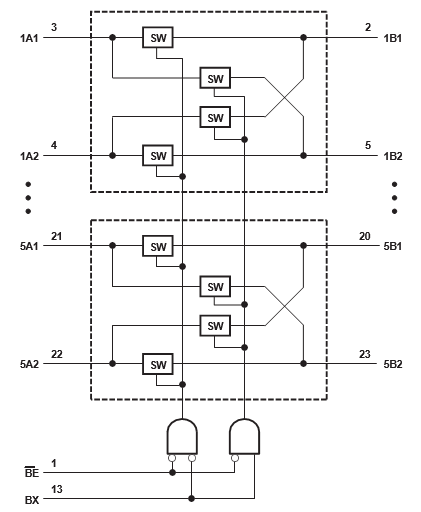
 Logic Diagram (Positive Logic)