-
THS4281 Very Low-Power, High-Speed, Rail-to-Rail Input and Output Voltage-Feedback Operational Amplifier
- 1 Features
- 2 Applications
- 3 Description
- 4 Revision History
- 5 Pin Configuration and Functions
-
6 Specifications
- 6.1 Absolute Maximum Ratings
- 6.2 ESD Ratings
- 6.3 Recommended Operating Conditions
- 6.4 Thermal Information
- 6.5 Electrical Characteristics, VS = 3 V (VS+ = 3 V, VS- = GND)
- 6.6 Electrical Characteristics, VS = 5 V (VS+ = 5 V, VS- = GND)
- 6.7 Electrical Characteristics, VS = ±5 V
- 6.8 Dissipation Ratings
- 6.9 Typical Characteristics
- 7 Detailed Description
- 8 Application and Implementation
- 9 Power Supply Recommendations
- 10Layout
- 11Device and Documentation Support
- 12Mechanical, Packaging, and Orderable Information
- IMPORTANT NOTICE
Package Options
Refer to the PDF data sheet for device specific package drawings
Mechanical Data (Package|Pins)
- D|8
- DBV|5
- DGK|8
Thermal pad, mechanical data (Package|Pins)
Orderable Information
THS4281 Very Low-Power, High-Speed, Rail-to-Rail Input and Output Voltage-Feedback Operational Amplifier
1 Features
- Very Low Quiescent Current: 750 μA (at 5 V)
- Rail-to-Rail Input and Output:
- Common-Mode Input Voltage Extends
400 mV Beyond the Rails - Output Swings Within 150 mV From the Rails
- Common-Mode Input Voltage Extends
- Wide –3-dB Bandwidth at 5 V:
- 90 MHz at Gain = +1, 40 MHz at Gain = +2
- High Slew Rate: 35 V/μs
- Fast Settling Time (2-V Step):
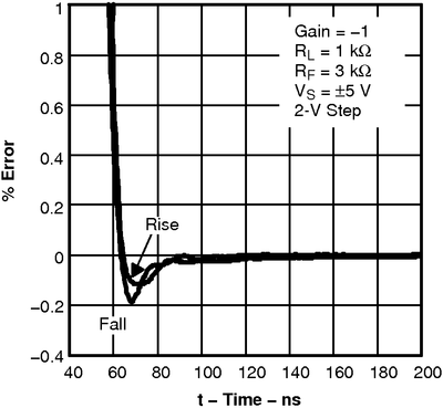
- 78 ns to 0.1%
- 150 ns to 0.01%
- Low Distortion at Gain = +2, VO = 2-VPP, 5 V:
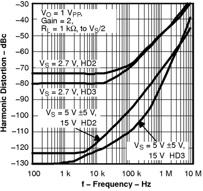
- –91 dBc at 100 kHz, –67 dBc at 1 MHz
- Input Offset Voltage: 2.5 mV (Max at +25°C)
- Output Current > 30 mA (10-Ω Load, 5 V)
- Low Voltage Noise of 12.5 nV/√Hz
- Supply Voltages: +2.7 V, 3 V, +5 V, ±5 V, +15 V
- Packages: SOT23, MSOP, and SOIC
2 Applications
- Portable/Battery-Powered Applications
- High Channel Count Systems
- ADC Buffer
- Active Filters
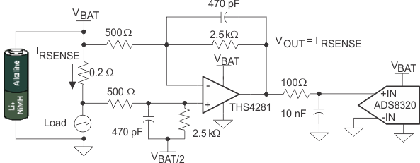
- Current Sensing
3 Description
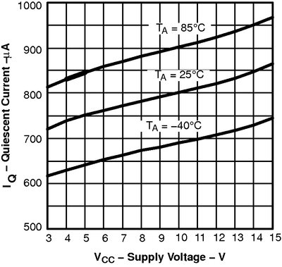
Fabricated using the BiCom-II process, the THS4281 is a low-power, rail-to-rail input and output, voltage-feedback operational amplifier designed to operate over a wide power-supply range of 2.7-V to 15-V single supply, and ±1.35-V to ±7.5-V dual supply. Consuming only 750 μA with a unity gain bandwidth of 90 MHz and a high 35-V/μs slew rate, the THS4281 allows portable or other power-sensitive applications to realize high performance with minimal power. To ensure long battery life in portable applications, the quiescent current is trimmed to be less than 900 μA at +25°C, and 1 mA from –40°C to +85°C.
The THS4281 is a true single-supply amplifier with a specified common-mode input range of 400 mV beyond the rails. This allows for high-side current sensing applications without phase reversal concerns. Its output swings to within 40 mV from the rails with 10-kΩ loads, and 150 mV from the rails with 1-kΩ loads.
The THS4281 has a good 0.1% settling time of 78 ns, and 0.01% settling time of 150 ns. The low THD of –87 dBc at 100 kHz, coupled with a maximum offset voltage of less than 2.5 mV, makes the THS4281 a good match for high-resolution ADCs sampling less than 2 MSPS.
The THS4281 is offered in a space-saving SOT23-5 package, a small MSOP-8 package, and the industry standard SOIC-8 package.
Device Information(1)
| PART NUMBER | PACKAGE | BODY SIZE (NOM) |
|---|---|---|
| THS4281 | SOIC (8) | 4.90 mm × 3.91 mm |
| SOT-23 (5) | 2.90 mm × 1.60 mm | |
| VSSOP (8) | 3.00 mm × 3.00 mm |
- For all available packages, see the orderable addendum at the end of the data sheet.
High-side, Low Power Current-Sensing system
4 Revision History
Changes from A Revision (November 2009) to B Revision
- Added Pin Configuration and Functions section, ESD Ratings table, Feature Description section, Device Functional Modes, Application and Implementation section, Power Supply Recommendations section, Layout section, Device and Documentation Support section, and Mechanical, Packaging, and Orderable Information section Go
- Removed the Packaging/Ordering Information table Go
- Removed Design Tools section Go
- Updated Thermal Values Go
- Removed the Applications Section Contents section Go
- Removed the Bill of Materials section Go
Changes from * Revision (April 2004) to A Revision
- Updated document format to current standardsGo
- Deleted Lead temperature specification from Absolute Maximum Ratings tableGo
- Revised Driving Capacitive Loads sectionGo
- Changed Board Layout section; revised statements in fourth recommendation about how to make connections to other wideband devices on the boardGo
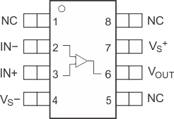
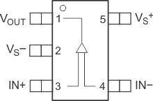
5 Pin Configuration and Functions
NOTE:
NC Indicates there is no internal connection to these pinsPin Functions
| PIN | I/O | DESCRIPTION | ||
|---|---|---|---|---|
| NAME | SOIC, VSSOP | SOT-23 | ||
| NC | 1 | — | — | |
| IN- | 2 | 4 | I | Negative input voltage pin |
| IN+ | 3 | 3 | I | Positive input voltage pin |
| Vs- | 4 | 2 | I/O | Negative supply input voltage pin |
| NC | 5 | — | — | |
| Vout | 6 | 1 | O | Output voltage pin |
| Vs+ | 7 | 5 | I/O | Postive supply input voltage pin |
| NC | 8 | — | — | |
6 Specifications
6.1 Absolute Maximum Ratings
Over operating free-air temperature range (unless otherwise noted).(1)| MIN | MAX | UNIT | ||
|---|---|---|---|---|
| Supply voltage, VS– to VS+ | 16.5 | V | ||
| Input voltage, VI | ±VS ± 0.5 | V | ||
| Differential input voltage, VID | ±2 | V | ||
| Output current, IO | ±100 | mA | ||
| Continuous power dissipation | See Dissipation Ratings Table | |||
| Maximum junction temperature, any condition, (2) TJ | +150 | °C | ||
| Maximum junction temperature, continuous operation, long-term reliability(2) TJ | 125° | °C | ||
| Storage temperature, Tstg | –65 | 150 | °C | |
6.2 ESD Ratings
| VALUE | UNIT | |||
|---|---|---|---|---|
| V(ESD) | Electrostatic discharge | Human-body model (HBM), per ANSI/ESDA/JEDEC JS-001(1) | ±3500 | V |
| Charged-device model (CDM), per JEDEC specification JESD22-C101(2) | ±1500 | |||
| Machine Model (MM) | ±100 | |||
6.3 Recommended Operating Conditions
| MIN | MAX | UNIT | ||
|---|---|---|---|---|
| Supply voltage, (VS+ and VS –) | Dual supply | ±1.35 | ±8.25 | V |
| Single supply | 2.7 | 16.5 | ||
6.4 Thermal Information
| THERMAL METRIC(1) | THS4281 | UNIT | |||
|---|---|---|---|---|---|
| DBV (SOT-23) | D (SOIC) | DGK (VSSOP) | |||
| 5 PINS | 8 PINS | 8 PINS | |||
| RθJA | Junction-to-ambient thermal resistance (2) | 154.4 | 126.6 | 192.5 | °C/W |
| RθJC(top) | Junction-to-case (top) thermal resistance | 115 | 69 | 77.7 | °C/W |
| RθJB | Junction-to-board thermal resistance | 31.4 | 64.7 | 112.8 | °C/W |
| ψJT | Junction-to-top characterization parameter | 14.7 | 20.5 | 14.6 | °C/W |
| ψJB | Junction-to-board characterization parameter | 31 | 64.3 | 111.3 | °C/W |
| RθJC(bot) | Junction-to-case (bottom) thermal resistance | N/A | N/A | N/A | °C/W |
6.5 Electrical Characteristics, VS = 3 V (VS+ = 3 V, VS– = GND)
At G = +2, RF = 2.49 kΩ, and RL = 1 kΩ to 1.5 V, TA = 25°C unless otherwise noted.| PARAMETER | TEST CONDITIONS | MIN | TYP | MAX | UNIT | ||
|---|---|---|---|---|---|---|---|
| AC PERFORMANCE | |||||||
| Small-Signal Bandwidth | G = +1, VO = 100 mVPP, RF = 34 Ω | 83 | MHz | ||||
| G = +2, VO = 100 mVPP, RF = 1.65 kΩ | 40 | MHz | |||||
| G = +5, VO = 100 mVPP, RF = 1.65 kΩ | 8 | MHz | |||||
| G = +10, VO = 100 mVPP, RF = 1.65 kΩ | 3.8 | MHz | |||||
| 0.1-dB Flat Bandwidth | G = +2, VO = 100 mVPP, RF = 1.65 kΩ | 20 | MHz | ||||
| Full-Power Bandwidth | G = +2, VO = 2 VPP | 8 | MHz | ||||
| Slew Rate | G = +1, VO = 2-V Step | 26 | V/μs | ||||
| G = –1, VO = 2-V Step | 27 | V/μs | |||||
| Settling time to 0.1% | G = –1, VO = 1-V Step | 80 | ns | ||||
| Settling time to 0.01% | G = –1, VO = 1-V Step | 155 | ns | ||||
| Rise/Fall Times | G = +1, VO = 2-V Step | 55 | ns | ||||
| AC PERFORMANCE— HARMONIC DISTORTION | |||||||
| Second Harmonic Distortion | G = +2, VO = 2 VPP, f = 1 MHz, RL = 1 kΩ | –52 | dBc | ||||
| G = +2, VO = 2 VPP, f = 100 kHz, RL = 1 kΩ | –52 | ||||||
| Third Harmonic Distortion | G = +2, VO = 2 VPP, f = 1 MHz, RL = 1 kΩ | –69 | dBc | ||||
| G = +2, VO = 2 VPP, f = 100 kHz, RL = 1 kΩ | –71 | ||||||
| THD + N | G = +2, VO = 2 VPP, VO = 1 VPP, f = 10 kHz | 0.003% | |||||
| G = +2, VO = 2 VPP, VO = 2 VPP, f = 10 kHz | 0.03% | ||||||
| Differential Gain (NTSC/PAL) | G = +2, RL = 150 Ω | 0.05/0.08% | |||||
| Differential Phase (NTSC/PAL) | G = +2, RL = 150 Ω | 0.25/0.35 | º | ||||
| Input Voltage Noise | f = 100 kHz | 12.5 | nA/√Hz | ||||
| Input Current Noise | f = 100 kHz | 1.5 | pA/√Hz | ||||
| DC PERFORMANCE | |||||||
| Open-Loop Voltage Gain (AOL) | 95 | dB | |||||
| Input Offset Voltage | VCM = 1.5 V | 25°C | 0.5 | 2.5 | mV | ||
| 0°C to 70°C | 3.5 | ||||||
| –40°C to +85°C | 3.5 | ||||||
| Average Offset Voltage Drift | VCM = 1.5 V | 0°C to 70°C | ±7 | µV/°C | |||
| –40°C to +85°C | ±7 | ||||||
| Input Bias Current | VCM = 1.5 V | 25°C | 0.5 | 0.8 | µA | ||
| 0°C to 70°C | 1 | ||||||
| –40°C to +85°C | 1 | ||||||
| Average Bias Current Drift | VCM = 1.5 V | 0°C to 70°C | ±2 | nA/°C | |||
| –40°C to +85°C | ±2 | ||||||
| Input Offset Current | VCM = 1.5 V | 25°C | 0.1 | 0.4 | μA | ||
| 0°C to 70°C | 0.5 | ||||||
| –40°C to +85°C | 0.5 | ||||||
| Average Offset Current Drift | VCM = 1.5 V | 0°C to 70°C | ±2 | nA/°C | |||
| –40°C to +85°C | ±2 | ||||||
| INPUT CHARACTERISTICS | |||||||
| Common-Mode Input Range | 25°C | –0.3/3.3 | –0.4/3.4 | V | |||
| 0°C to 70°C | –0.1/3.1 | ||||||
| –40°C to +85°C | –0.1/3.1 | ||||||
| Common-Mode Rejection Ratio | VCM = 0 V to 3 V | 25°C | 75 | 92 | dB | ||
| 0°C to 70°C | 70 | ||||||
| –40°C to +85°C | 70 | ||||||
| Input Resistance | Common-mode | 100 | MΩ | ||||
| Input Capacitance | Common-mode/Differential | 0.8/1.2 | pF | ||||
| OUTPUT CHARACTERISTICS | |||||||
| Output Voltage Swing | RL = 10 kΩ | 0.04/2.96 | V | ||||
| RL = 1 kΩ | 25°C | 0.14/2.86 | 0.1/2.9 | V | |||
| 0°C to 70°C | 0.2/2.8 | ||||||
| –40°C to +85°C | 0.2/2.8 | ||||||
| Output Current (Sourcing) | RL = 10 Ω | 25°C | 18 | 23 | mA | ||
| 0°C to 70°C | 15 | ||||||
| –40°C to +85°C | 15 | ||||||
| Output Current (Sinking) | RL = 10 Ω | 25°C | 22 | 29 | mA | ||
| 0°C to 70°C | 19 | ||||||
| –40°C to +85°C | 19 | ||||||
| Output Impedance | f = 1 MHz | 1 | Ω | ||||
| POWER SUPPLY | |||||||
| Maximum Operating Voltage | 25°C | 3 | 16.5 | V | |||
| 0°C to 70°C | 16.5 | ||||||
| –40°C to +85°C | 16.5 | ||||||
| Minimum Operating Voltage | 25°C | 2.7 | 3 | V | |||
| 0°C to 70°C | 2.7 | ||||||
| –40°C to +85°C | 2.7 | ||||||
| Maximum Quiescent Current | 25°C | 0.75 | 0.9 | mA | |||
| 0°C to 70°C | 0.98 | ||||||
| –40°C to +85°C | 1 | ||||||
| Minimum Quiescent Current | 25°C | 0.6 | 0.75 | mA | |||
| 0°C to 70°C | 0.57 | ||||||
| –40°C to +85°C | 0.55 | ||||||
| Power-Supply Rejection (+PSRR) | VS+ = 3.25 V to 2.75 V, VS– = 0 V | 25°C | 70 | 90 | dB | ||
| 0°C to 70°C | 65 | ||||||
| –40°C to +85°C | 65 | ||||||
| Power-Supply Rejection (–PSRR) | VS+ = 3 V, VS– = 0 V to 0.65 V | 25°C | 70 | 90 | dB | ||
| 0°C to 70°C | 65 | ||||||
| –40°C to +85°C | 65 | ||||||
6.6 Electrical Characteristics, VS = 5 V (VS+ = 5 V, VS– = GND)
At G = +2, RF = 2.49 kΩ, and RL = 1 kΩ to 2.5 V, TA = 25°C unless otherwise noted.| PARAMETER | TEST CONDITIONS | MIN | TYP | MAX | UNIT | ||
|---|---|---|---|---|---|---|---|
| AC PERFORMANCE | |||||||
| Small-Signal Bandwidth | G = +1, VO = 100 mVPP, RF = 34 Ω | 90 | MHz | ||||
| G = +2, VO = 100 mVPP, RF = 2 kΩ | 40 | MHz | |||||
| G = +5, VO = 100 mVPP, RF = 2 kΩ | 8 | MHz | |||||
| G = +10, VO = 100 mVPP, RF = 2 kΩ | 3.8 | MHz | |||||
| 0.1-dB Flat Bandwidth | G = +2, VO = 100 mVPP, RF = 2 kΩ | 20 | MHz | ||||
| Full-Power Bandwidth | G = +2, VO = 2 VPP | 9 | MHz | ||||
| Slew Rate | G = +1, VO = 2-V Step | 31 | V/μs | ||||
| G = –1, VO = 2-V Step | 34 | V/μs | |||||
| Settling Time to 0.1% | G = –1, VO = 2-V Step | 78 | ns | ||||
| Settling Time to 0.01% | G = –1, VO = 2-V Step | 150 | ns | ||||
| Rise/Fall Times | G = +1, VO = 2-V Step | 48 | ns | ||||
| AC PERFORMANCE— HARMONIC DISTORTION | |||||||
| Second Harmonic Distortion | G = +2, VO = 2 VPP, f = 1 MHz, RL = 1 kΩ | –67 | dBc | ||||
| G = +2, VO = 2 VPP, f = 100 kHz, RL = 1 kΩ | –92 | ||||||
| Third Harmonic Distortion | G = +2, VO = 2 VPP, f = 1 MHz, RL = 1 kΩ | –76 | dBc | ||||
| G = +2, VO = 2 VPP, f = 100 kHz, RL = 1 kΩ | –106 | ||||||
| THD + N | G = +2, VO = 2 VPP, VO = 2 VPP, f = 10 kHz | 0.0009% | |||||
| G = +2, VO = 2 VPP, VO = 4 VPP, f = 10 kHz | 0.0005% | ||||||
| Differential Gain (NTSC/PAL) | G = +2, RL = 150 Ω | 0.11/0.17% | |||||
| Differential Phase (NTSC/PAL) | 0.11/0.14 | º | |||||
| Input Voltage Noise | f = 100 kHz | 12.5 | nV/√Hz | ||||
| Input Current Noise | f = 100 kHz | 1.5 | pA/√Hz | ||||
| DC PERFORMANCE | |||||||
| Open-Loop Voltage Gain (AOL) | 25°C | 85 | 105 | dB | |||
| 0°C to 70°C | 80 | ||||||
| –40°C to +85°C | 80 | ||||||
| Input Offset Voltage | VCM = 2.5 V | 25°C | 2.5 | 0.5 | mV | ||
| 0°C to 70°C | 3.5 | ||||||
| –40°C to +85°C | 3.5 | ||||||
| Average Offset Voltage Drift | VCM = 2.5 V | 0°C to 70°C | ±7 | µV/°C | |||
| –40°C to +85°C | ±7 | ||||||
| Input Bias Current | VCM = 2.5 V | 25°C | 0.5 | 0.8 | µA | ||
| 0°C to 70°C | 1 | ||||||
| –40°C to +85°C | 1 | ||||||
| Average Bias Current Drift | VCM = 2.5 V | 0°C to 70°C | ±2 | nA/°C | |||
| –40°C to +85°C | ±2 | ||||||
| Input Offset Current | VCM = 2.5 V | 25°C | 0.1 | 0.4 | µA | ||
| 0°C to 70°C | 0.5 | ||||||
| –40°C to +85°C | 0.5 | ||||||
| Average Offset Current Drift | VCM = 2.5 V | 0°C to 70°C | ±2 | nA/°C | |||
| –40°C to +85°C | ±2 | ||||||
| INPUT CHARACTERISTICS | |||||||
| Common-Mode Input Range | 25°C | –0.4/5.4 | –0.3/5.3 | V | |||
| 0°C to 70°C | –0.1/5.1 | ||||||
| –40°C to +85°C | –0.1/5.1 | ||||||
| Common-Mode Rejection Ratio | VCM = 0 V to 5 V | 25°C | 85 | 100 | dB | ||
| 0°C to 70°C | 80 | ||||||
| –40°C to +85°C | 80 | ||||||
| Input Resistance | Common-mode | 100 | MΩ | ||||
| Input Capacitance | Common-mode/Differential | 0.8/1.2 | pF | ||||
| OUTPUT CHARACTERISTICS | |||||||
| Output Voltage Swing | RL = 10 kΩ | 0.04/4.96 | V | ||||
| RL = 1 kΩ | 25°C | 0.2/4.8 | 0.15/4.85 | V | |||
| 0°C to 70°C | 0.25/4.75 | ||||||
| –40°C to +85°C | 0.25/4.75 | ||||||
| Output Current (Sourcing) | RL = 10 Ω | 25°C | 24 | 33 | mA | ||
| 0°C to 70°C | 20 | ||||||
| –40°C to +85°C | 20 | ||||||
| Output Current (Sinking) | RL = 10 Ω | 25°C | 30 | 44 | mA | ||
| 0°C to 70°C | 25 | ||||||
| –40°C to +85°C | 25 | ||||||
| Output Impedance | f = 1 MHz | 25°C | 1 | Ω | |||
| 0°C to 70°C | |||||||
| –40°C to +85°C | |||||||
| POWER SUPPLY | |||||||
| Maximum Operating Voltage | 25°C | 5 | 16.5 | V | |||
| 0°C to 70°C | 16.5 | ||||||
| –40°C to +85°C | 16.5 | ||||||
| Minimum Operating Voltage | 25°C | 2.7 | 5 | V | |||
| 0°C to 70°C | 2.7 | ||||||
| –40°C to +85°C | 2.7 | ||||||
| Maximum Quiescent Current | 25°C | 0.75 | 0.9 | mA | |||
| 0°C to 70°C | 0.98 | ||||||
| –40°C to +85°C | 1.0 | ||||||
| Minimum Quiescent Current | 25°C | 0.6 | 0.75 | mA | |||
| 0°C to 70°C | 0.57 | ||||||
| –40°C to +85°C | 0.55 | ||||||
| Power-Supply Rejection (+PSRR) | VS+ = 5.5 V to 4.5 V, VS– = 0 V | 25°C | 80 | 100 | dB | ||
| 0°C to 70°C | 75 | ||||||
| –40°C to +85°C | 75 | ||||||
| Power-Supply Rejection (–PSRR) | VS+ = 5 V, VS– = 0 V to 1.0 V | 25°C | 80 | 100 | dB | ||
| 0°C to 70°C | 75 | ||||||
| –40°C to +85°C | 75 | ||||||
6.7 Electrical Characteristics, VS = ±5 V
At G = +2, RF = 2.49 kΩ, and RL = 1 kΩ, unless otherwise noted| PARAMETER | TEST CONDITIONS | MIN | TYP | MAX | UNIT | ||||
|---|---|---|---|---|---|---|---|---|---|
| AC PERFORMANCE | |||||||||
| Small-Signal Bandwidth | G = +1, VO = 100 mVPP, RF = 34 Ω | 95 | MHz | ||||||
| G = +2, VO = 100 mVPP | 40 | MHz | |||||||
| G = +5, VO = 100 mVPP | 8 | MHz | |||||||
| G = +10, VO = 100 mVPP | 3.8 | MHz | |||||||
| 0.1-dB Flat Bandwidth | G = +2, VO = 100 mVPP | 20 | MHz | ||||||
| Full-Power Bandwidth | G = +1, VO = 2 VPP | 9.5 | MHz | ||||||
| Slew Rate | G = +1, VO = 2-V Step | 35 | V/μs | ||||||
| G = –1, VO = 2-V Step | 35 | V/μs | |||||||
| Settling Time to 0.1% | G = –1, VO = 2-V Step | 78 | ns | ||||||
| Settling Time to 0.01% | G = –1, VO = 2-V Step | 140 | ns | ||||||
| Rise/Fall Times | G = +1, VO = 2-V Step | 45 | ns | ||||||
| AC PERFORMANCE— HARMONIC DISTORTION | |||||||||
| Second Harmonic Distortion | G = +2, VO = 2 VPP, f = 1 MHz, RL = 1 kΩ | –69 | dBc | ||||||
| G = +2, VO = 2 VPP, f = 100 kHz, RL = 1 kΩ | –76 | ||||||||
| Third Harmonic Distortion | G = +2, VO = 2 VPP, f = 1 MHz, RL = 1 kΩ | –93 | dBc | ||||||
| G = +2, VO = 2 VPP, f = 100 kHz, RL = 1 kΩ | –107 | ||||||||
| THD + N | G = +2, VO = 2 VPP, VO = 2 VPP, f = 10 kHz | 0.0009 | |||||||
| G = +2, VO = 2 VPP, VO = 4 VPP, f = 10 kHz | 0.0003% | ||||||||
| Differential Gain (NTSC/PAL) | G = +2, RL = 150 Ω | 0.03/0.03% | |||||||
| Differential Phase (NTSC/PAL) | 0.08/0.1 | º | |||||||
| Input Voltage Noise | f = 100 kHz | 12.5 | nV/√Hz | ||||||
| Input Current Noise | f = 100 kHz | 1.5 | pA/√Hz | ||||||
| DC PERFORMANCE | |||||||||
| Open-Loop Voltage Gain (AOL) | 25°C | 90 | 108 | dB | |||||
| 0°C to 70°C | 85 | ||||||||
| –40°C to +85°C | 85 | ||||||||
| Input Offset Voltage | VCM = 0 V | 25°C | 0.5 | 2.5 | mV | ||||
| 0°C to 70°C | 3.5 | ||||||||
| –40°C to +85°C | 3.5 | ||||||||
| Average Offset Voltage Drift | VCM = 0 V | 0°C to 70°C | ±7 | μV/°C | |||||
| –40°C to +85°C | ±7 | ||||||||
| Input Bias Current | VCM = 0 V | 25°C | 0.5 | 0.8 | μA | ||||
| 0°C to 70°C | 1 | ||||||||
| –40°C to +85°C | 1 | ||||||||
| Average Bias Current Drift | VCM = 0 V | 0°C to 70°C | ±2 | nA/°C | |||||
| –40°C to +85°C | ±2 | ||||||||
| Input Offset Current | VCM = 0 V | 25°C | 0.1 | 0.4 | μA | ||||
| 0°C to 70°C | 0.5 | ||||||||
| –40°C to +85°C | 0.5 | ||||||||
| Average Offset Current Drift | VCM = 0 V | 0°C to 70°C | ±2 | nA/°C | |||||
| –40°C to +85°C | ±2 | ||||||||
| INPUT CHARACTERISTICS | |||||||||
| Common-Mode Input Range | 25°C | ±5.3 | ±5.4 | V | |||||
| 0°C to 70°C | ±5.1 | ||||||||
| –40°C to +85°C | ±5.1 | ||||||||
| Common-Mode Rejection Ratio | VCM = –5 V to +5 V | 25°C | 90 | 107 | dB | ||||
| 0°C to 70°C | 85 | ||||||||
| –40°C to +85°C | 85 | ||||||||
| Input Resistance | Common-mode | 100 | MΩ | ||||||
| Input Capacitance | Common-mode/Differential | 0.8/1.2 | pF | ||||||
| OUTPUT CHARACTERISTICS | |||||||||
| Output Voltage Swing | RL = 10 kΩ | ±4.93 | V | ||||||
| RL = 1 kΩ | 25°C | ±4.6 | ±4.8 | V | |||||
| 0°C to 70°C | ±4.5 | ||||||||
| –40°C to +85°C | ±4.5 | ||||||||
| Output Current (Sourcing) | RL = 10 Ω | 25°C | 35 | 48 | mA | ||||
| 0°C to 70°C | 30 | ||||||||
| –40°C to +85°C | 30 | ||||||||
| Output Current (Sinking) | RL = 10 Ω | 25°C | 45 | 60 | mA | ||||
| 0°C to 70°C | 40 | ||||||||
| –40°C to +85°C | 40 | ||||||||
| Output Impedance | f = 1 MHz | 1 | Ω | ||||||
| POWER SUPPLY | |||||||||
| Maximum Operating Voltage | 25°C | ±5 | ±8.25 | V | |||||
| 0°C to 70°C | ±8.25 | ||||||||
| –40°C to +85°C | ±8.25 | ||||||||
| Minimum Operating Voltage | 25°C | ±1.35 | ±5 | V | |||||
| 0°C to 70°C | ±1.35 | ||||||||
| –40°C to +85°C | ±1.35 | ||||||||
| Maximum Quiescent Current | 25°C | 0.8 | 0.93 | mA | |||||
| 0°C to 70°C | 1.0 | ||||||||
| –40°C to +85°C | 1.05 | ||||||||
| Minimum Quiescent Current | 25°C | 0.67 | 0.8 | mA | |||||
| 0°C to 70°C | 0.62 | ||||||||
| –40°C to +85°C | 0.6 | ||||||||
| Power-Supply Rejection (+PSRR) | VS+ = 5.5 V to 4.5 V, VS– = 5.0 V | 25°C | 80 | 100 | dB | ||||
| 0°C to 70°C | 75 | ||||||||
| –40°C to +85°C | 75 | ||||||||
| Power-Supply Rejection (–PSRR) | VS+ = 5 V, VS– = –5.5 V to –4.5 V | 25°C | 80 | 100 | dB | ||||
| 0°C to 70°C | 75 | ||||||||
| –40°C to +85°C | 75 | ||||||||
6.8 Dissipation Ratings
| PACKAGE | POWER RATING(1) | |
|---|---|---|
| TA < +25°C | TA = +85°C | |
| DBV (5) | 391 mW | 156 mW |
| D (8) | 1.02 W | 410 mW |
| DGK (8) | 553 mW | 221 mW |
6.9 Typical Characteristics

| VS = ±5 V |
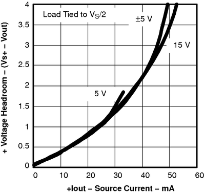
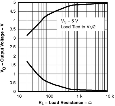
| VS = 5 V |
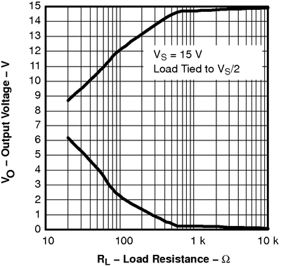
| VS = 15 V) | ||
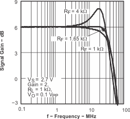
| VS = 2.7 V |
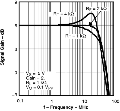
| VS = 5 V |
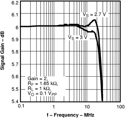
| VS = 2.7 V | VS = 3 V |

| VS = 2.7 V |
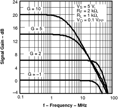
| VS = 5 V |
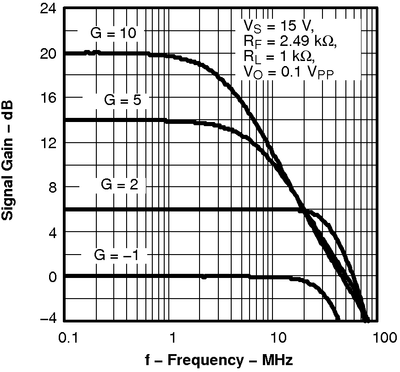
| VS = 15 V |
| VS = 5 V | ||
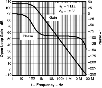 Figure 25. Open-Loop Gain vs Frequency
| VS = 2.7 V |
| VS = ±5 V |
| VS = ±1.35 V |

| VS = ±2.5 V |
| VS = ±5 V |
| Gain = +1 |
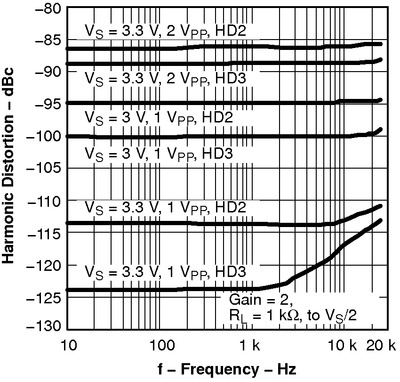
| VS = 3 V, 3.3 V |
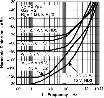
| Gain = +2 | ||
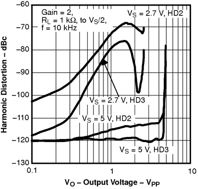
| VS = 2.7 V, 5 V | ||
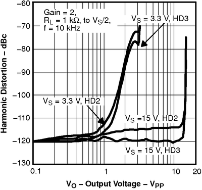
| VS = 3.3 V, 15 V | ||
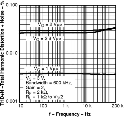
| VS = 3 V | ||
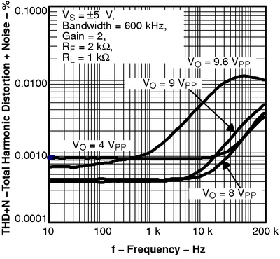
| VS = ±5 V | ||
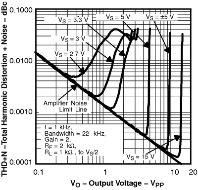
| f = 1 kHz | ||
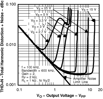
| f = 100 kHz | ||
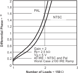
| VS = 5 V |
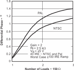
| VS = ±5 V | ||
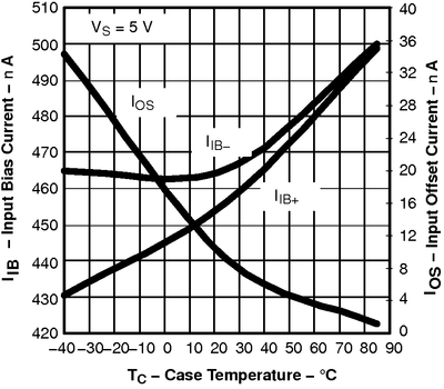
| VS = 5 V | ||
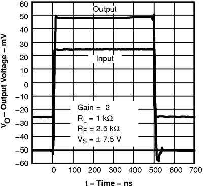
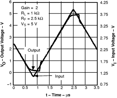
| VS = 5 V | ||
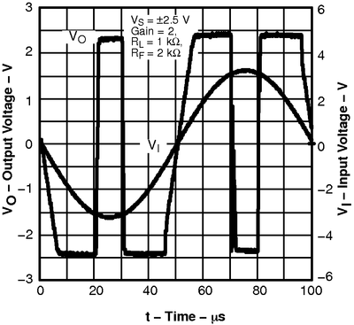
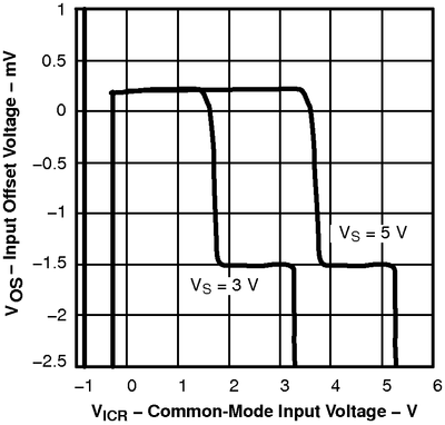
| VS = 3 V | VS = 5 V |
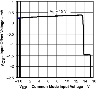
| VS = 15 V |
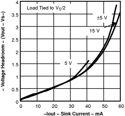
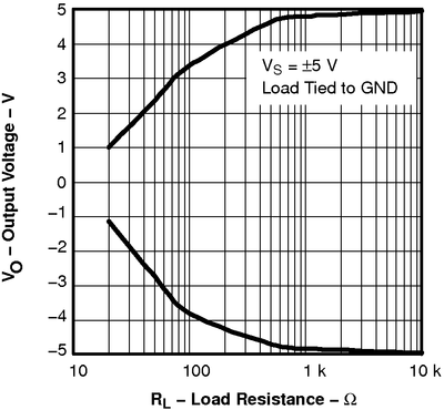
| VS = ±5 V |
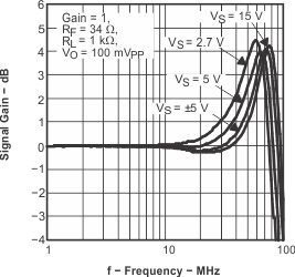
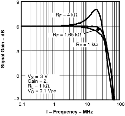
| VS = 3 V |
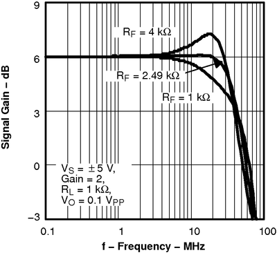
| VS = ±5 V |
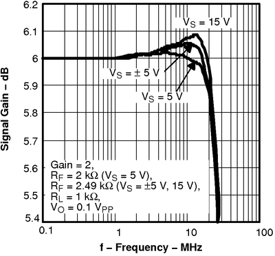
| VS = 5 V, ±5 V, 15 V |
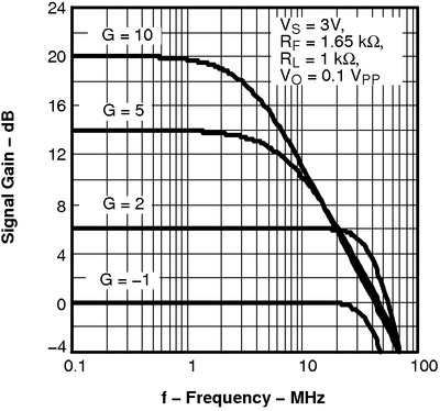
| VS = 3 V |
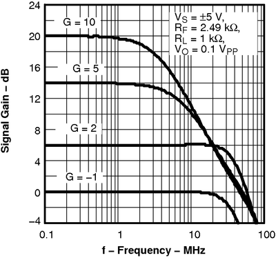
| VS = ±5 V |
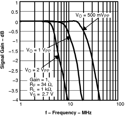
| VS = 2.7 V |
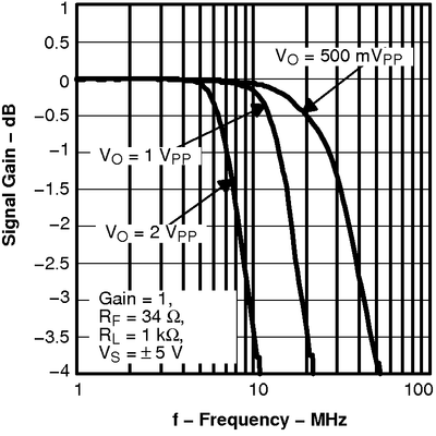
| VS = ±5 V | ||
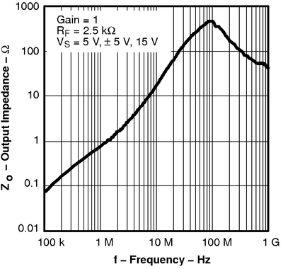 Figure 26. Output Impedance vs Frequency
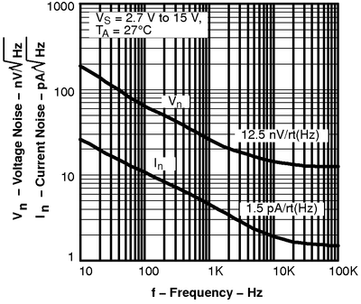
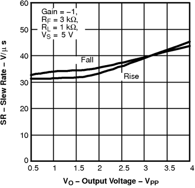
| VS = 5 V |
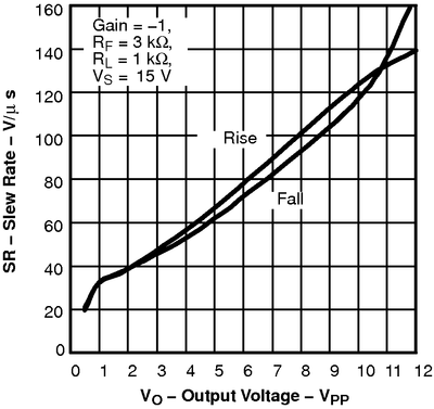
| VS = 15 V |
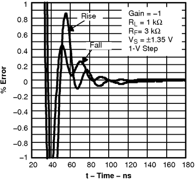
| VS = ±1.35 V |
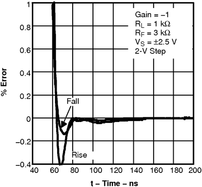
| VS = ±2.5 V |
| VS = ±5 V |

| Gain = +1 |
| Gain = +2 |
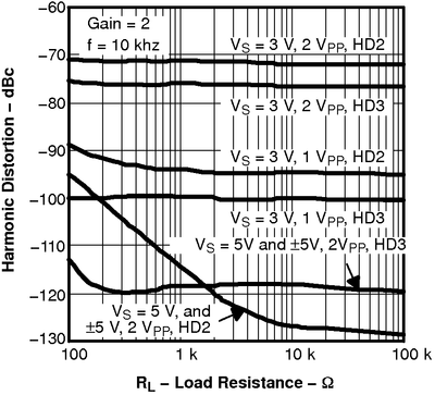 Figure 44. Harmonic Distortion vs Load Resistance
| VS = 3 V, ±5 V | ||
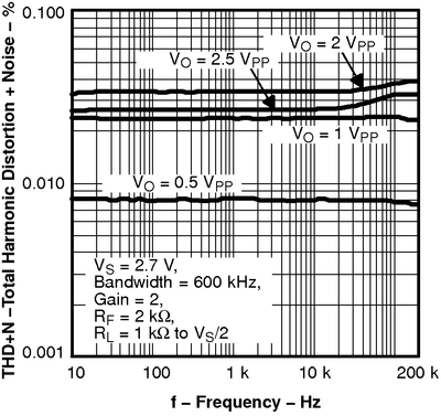
| VS = 2.7 V | ||
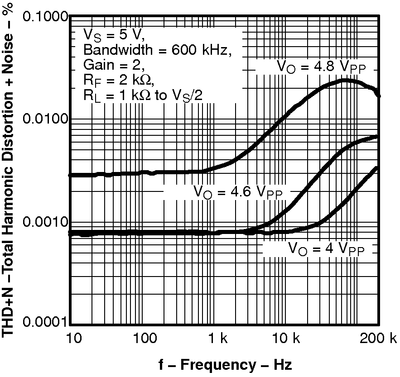
| VS = 5 V | ||
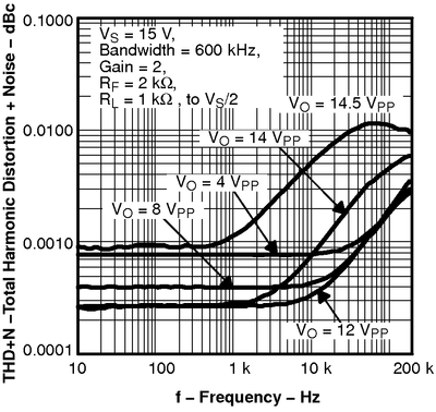
| VS = 15 V | ||
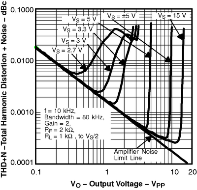
| f = 10 kHz | ||
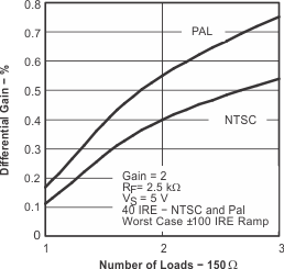
| VS = 5 V | ||
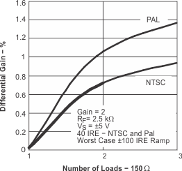
| VS = ±5 V | ||

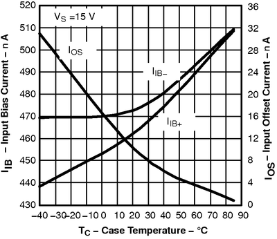
| VS = 15 V | ||
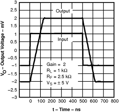
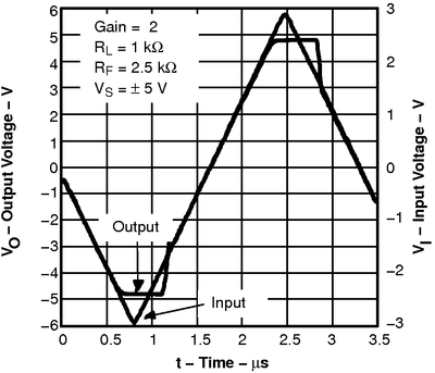
| VS = ±5 V | ||
7 Detailed Description
7.1 Overview
7.2 Feature Description
7.2.1 Wideband, Noninverting Operation
Figure 68 shows the noninverting gain configuration of 2 V/V used to demonstrate the typical performance curves.
Voltage feedback amplifiers can use a wide range of resistors values to set their gain with minimal impact on frequency response. Larger-valued resistors decrease loading of the feedback network on the output of the amplifier, but may cause peaking and instability. For a gain of +2, feedback resistor values between 1 kΩ and 4 kΩ are recommended for most applications. However, as the gain increases, the use of even higher feedback resistors can be used to conserve power. This is due to the inherent nature of amplifiers becoming more stable as the gain increases, at the expense of bandwidth. Figure 73 and Figure 74 show the THS4281 using feedback resistors of 10 kΩ and 100 kΩ. Be cautioned that using such high values with high-speed amplifiers is not typically recommended, but under certain conditions, such as high gain and good high-speed printed circuit board (PCB) layout practices, such resistances can be used.
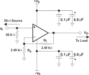 Figure 68. Wideband, Noninverting Gain Configuration
7.2.2 Wideband, Inverting Operation
Figure 69 shows a typical inverting configuration where the input and output impedances and noise gain from Figure 68 are retained with an inverting circuit gain of –1 V/V.
 Figure 69. Wideband, Inverting Gain Configuration
In the inverting configuration, some key design considerations must be noted. One is that the gain resistor (Rg) becomes part of the signal channel input impedance. If the input impedance matching is desired (which is beneficial whenever the signal is coupled through a cable, twisted pair, long PCB trace, or other transmission line conductors), Rg may be set equal to the required termination value and Rf adjusted to give the desired gain. However, care must be taken when dealing with low inverting gains, as the resulting feedback resistor value can present a significant load to the amplifier output. For example, an inverting gain of 2, setting Rg to 49.9 Ω for input matching, eliminates the need for RM but requires a 100-Ω feedback resistor. The 100-Ω feedback resistor, in parallel with the external load, causes excessive loading on the amplifier output. To eliminate this excessive loading, it is preferable to increase both Rg and Rf values, as shown in Figure 69, and then achieve the input matching impedance with a third resistor (RM) to ground. The total input impedance is the parallel combination of Rg and RM.
Another consideration in inverting amplifier design is setting the bias current cancellation resistor (RT) on the noninverting input. If the resistance is set equal to the total dc resistance presented to the device at the inverting terminal, the output dc error (due to the input bias currents) is reduced to the input offset current multiplied by RT. In Figure 69, the dc source impedance presented at the inverting terminal is 2.49 kΩ || (2.49 kΩ + 25.3 Ω) ≈ 1.24 kΩ. To reduce the additional high-frequency noise introduced by the resistor at the noninverting input, RT is bypassed with a 0.1-μF capacitor to ground (CT).
7.3 Device Functional Modes
This device has no specific function modes.