SLVSER5A December 2018 – May 2021 TPS73801-SEP
PRODUCTION DATA
- 1 Features
- 2 Applications
- 3 Description
- 4 Revision History
- 5 Pin Configuration and Functions
- 6 Specifications
- 7 Detailed Description
- 8 Application and Implementation
- 9 Power Supply Recommendations
- 10Layout
- 11Device and Documentation Support
- 12Mechanical, Packaging, and Orderable Information
Package Options
Mechanical Data (Package|Pins)
- DCQ|6
Thermal pad, mechanical data (Package|Pins)
Orderable Information
1 Features
- VID V62/18616
- Radiation hardened
- SEL, SEB, and SEGR immune up to
LET = 43 MeV-cm2/mg - SET and SEFI characterized up to
LET = 43 MeV-cm2/mg - TID assured for every
wafer lot up to
20 krad(Si) - TID characterized up to 50 krad(Si)
- SEL, SEB, and SEGR immune up to
- Space enhanced plastic
- Au bondwire and NiPdAu lead finish
- Enhanced mold compound for low outgassing
- One fabrication, assembly, and test site
- Extended product life cycle
- Extended product change notification
- Product traceability
- Optimized for fast transient response
- Output current: 1 A
- Dropout voltage: 300 mV
- Low noise: 45 µVRMS (10 Hz to 100 kHz)
- 1-mA quiescent current
- No protection diodes needed
- Controlled quiescent current in dropout
- Adjustable output voltage: 1.21 V to 20 V
- Less than 1-µA quiescent current in shutdown
- Stable with 10-µF output capacitor
- Stable with ceramic capacitors
- Reverse-battery protection
- No reverse current
- Thermal limiting
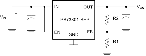
 Simplified Schematic