SNAS305J July 2005 – March 2016 ADC121S021
PRODUCTION DATA.
- 1 Features
- 2 Applications
- 3 Description
- 4 Revision History
- 5 Device Comparison Table
- 6 Pin Configuration and Functions
- 7 Specifications
- 8 Parameter Measurement Information
- 9 Detailed Description
- 10Applications Information
- 11Power Supply Recommendations
- 12Layout
- 13Device and Documentation Support
- 14Mechanical, Packaging, and Orderable Information
9 Detailed Description
9.1 Overview
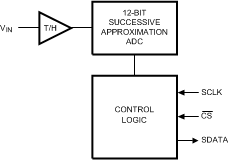
The ADC121S021 is a low-power, single-channel, 12-bit analog-to-digital converter which is based upon a successive-approximation register architecture with an internal track-and-hold circuit. It operates with a single‑supply voltage that can range from 2.7 V to 5.25 V. The ADC121S021 is packaged in 6-pin WSON and SOT-23 package. Operation over the industrial temperature range of –40⁰C to 85⁰C is ensured.
9.2 Functional Block Diagram

9.3 Feature Description
The ADC121S021 is fully specified over a sample rate range of 50 ksps to 200 ksps. Normal power consumption of the device using a 3.6-V or 5.25-V supply is 1.5 mW and 7.9 mW, respectively. The power-down feature helps reduce the power consumption to as low as 2.6 µW using a 5.25-V supply. The output serial data is straight binary, and is compatible with several standards such as SPI, QSPI, MICROWIRE, and many common DSP serial interfaces.
9.4 Device Functional Modes
The ADC has two possible modes of operation: normal mode, and shutdown mode. The ADC enters normal mode (and a conversion process is begun) when CS is pulled low. The device enters shutdown mode if CS is pulled high before the 10th falling edge of SCLK after CS is pulled low, or stays in normal mode if CS remains low. When in shutdown mode, the device stays there until CS is brought low again. By varying the ratio of time spent in the normal and shutdown modes, a system may trade off throughput for power consumption, with a sample rate as low as zero.
9.4.1 Normal Mode
The fastest possible throughput is obtained by leaving the ADC in normal mode at all times, so there are no power-up delays. To keep the device in normal mode continuously, CS must be kept low until after the 10th falling edge of SCLK after the start of a conversion (remember that a conversion is initiated by bringing CS low).
If CS is brought high after the 10th falling edge, but before the 16th falling edge, the device remains in normal mode, but the current conversion aborts, and SDATA returns to TRI-STATE (truncating the output word).
Sixteen SCLK cycles are required to read all of a conversion word from the device. After sixteen SCLK cycles have elapsed, CS may be idled either high or low until the next conversion. If CS is idled low, it must be brought high again before the start of the next conversion, which begins when CS is again brought low.
After sixteen SCLK cycles, SDATA returns to TRI-STATE. Another conversion may be started, after tQUIET has elapsed, by bringing CS low again.
9.4.2 Shutdown Mode
Shutdown mode is appropriate for applications that either do not sample continuously, or it is acceptable to trade throughput for power consumption. When the ADC is in shutdown mode, all of the analog circuitry is turned off.
To enter shutdown mode, a conversion must be interrupted by bringing CS high anytime between the second and 10th falling edges of SCLK, as shown in Figure 13. Once CS has been brought high in this manner, the device enters shutdown mode; the current conversion is aborted and SDATA enters TRI-STATE. If CS is brought high before the second falling edge of SCLK, the device does not change mode; this is to avoid accidentally changing mode as a result of noise on the CS line.
 Figure 13. Entering Shutdown Mode
 Figure 14. Entering Normal Mode
To exit shutdown mode, bring CS back low. Upon bringing CS low, the ADC begins powering up (power-up time is specified in Timing Requirements). This power-up delay results in the first conversion result being unusable. The second conversion performed after power-up, however, is valid, as shown in Figure 14.
If CS is brought back high before the 10th falling edge of SCLK, the device returns to shutdown mode. This is done to avoid accidentally entering normal mode as a result of noise on the CS line. To exit shutdown mode and remain in normal mode, CS must be kept low until after the 10th falling edge of SCLK. The ADC is fully powered up after 16 SCLK cycles.