ZHCSFU8B May 2016 – December 2021 ADC32RF80 , ADC32RF83
PRODUCTION DATA
- 1 特性
- 2 应用
- 3 说明
- 4 Revision History
- 5 Pin Configuration and Functions
-
6 Specifications
- 6.1 Absolute Maximum Ratings
- 6.2 ESD Ratings
- 6.3 Recommended Operating Conditions
- 6.4 Thermal Information
- 6.5 Electrical Characteristics
- 6.6 AC Performance Characteristics: fS = 2949.12 MSPS
- 6.7 AC Performance Characteristics: fS = 2457.6 MSPS (Performance Optimized for F + A + D Band)
- 6.8 AC Performance Characteristics: fS = 2457.6 MSPS (Performance Optimized for F + A Band)
- 6.9 Digital Requirements
- 6.10 Timing Requirements
- 6.11 Typical Characteristics
- 7 Parameter Measurement Information
-
8 Detailed Description
- 8.1 Overview
- 8.2 Functional Block Diagram
- 8.3
Feature Description
- 8.3.1 Analog Inputs
- 8.3.2 Clock Input
- 8.3.3 SYSREF Input
- 8.3.4 DDC Block
- 8.3.5 NCO Switching
- 8.3.6 SerDes Transmitter Interface
- 8.3.7 Eye Diagrams
- 8.3.8 Alarm Outputs: Power Detectors for AGC Support
- 8.3.9 Power-Down Mode
- 8.3.10 ADC Test Pattern
- 8.4
Device Functional Modes
- 8.4.1 Device Configuration
- 8.4.2
JESD204B Interface
- 8.4.2.1 JESD204B Initial Lane Alignment (ILA)
- 8.4.2.2 JESD204B Frame Assembly
- 8.4.2.3 JESD204B Frame Assembly with Decimation (Single-Band DDC): Complex Output
- 8.4.2.4 JESD204B Frame Assembly with Decimation (Single-Band DDC): Real Output
- 8.4.2.5 JESD204B Frame Assembly with Decimation (Single-Band DDC): Real Output
- 8.4.2.6 JESD204B Frame Assembly with Decimation (Dual-Band DDC): Complex Output
- 8.4.2.7 JESD204B Frame Assembly with Decimation (Dual-Band DDC): Real Output
- 8.4.3 Serial Interface
- 8.5
Register Maps
- 8.5.1 Example Register Writes
- 8.5.2
Register Descriptions
- 8.5.2.1
General Registers
- 8.5.2.1.1 Register 000h (address = 000h), General Registers
- 8.5.2.1.2 Register 002h (address = 002h), General Registers
- 8.5.2.1.3 Register 003h (address = 003h), General Registers
- 8.5.2.1.4 Register 004h (address = 004h), General Registers
- 8.5.2.1.5 Register 010h (address = 010h), General Registers
- 8.5.2.1.6 Register 011h (address = 011h), General Registers
- 8.5.2.1.7 Register 012h (address = 012h), General Registers
- 8.5.2.1
General Registers
- 8.5.3
Master Page (M = 0)
- 8.5.3.1 Register 020h (address = 020h), Master Page
- 8.5.3.2 Register 032h (address = 032h), Master Page
- 8.5.3.3 Register 039h (address = 039h), Master Page
- 8.5.3.4 Register 03Ch (address = 03Ch), Master Page
- 8.5.3.5 Register 05Ah (address = 05Ah), Master Page
- 8.5.3.6 Register 03Dh (address = 3Dh), Master Page
- 8.5.3.7 Register 057h (address = 057h), Master Page
- 8.5.3.8 Register 058h (address = 058h), Master Page
- 8.5.4 ADC Page (FFh, M = 0)
- 8.5.5 Digital Function Page (610000h, M = 1 for Channel A and 610100h, M = 1 for Channel B)
- 8.5.6 Offset Corr Page Channel A (610000h, M = 1)
- 8.5.7 Offset Corr Page Channel B (610000h, M = 1)
- 8.5.8 Digital Gain Page (610005h, M = 1 for Channel A and 610105h, M = 1 for Channel B)
- 8.5.9 Main Digital Page Channel A (680000h, M = 1)
- 8.5.10 Main Digital Page Channel B (680001h, M = 1)
- 8.5.11
JESD Digital Page (6900h, M = 1)
- 8.5.11.1 Register 001h (address = 001h), JESD Digital Page
- 8.5.11.2 Register 002h (address = 002h ), JESD Digital Page
- 8.5.11.3 Register 003h (address = 003h), JESD Digital Page
- 8.5.11.4 Register 004h (address = 004h), JESD Digital Page
- 8.5.11.5 Register 006h (address = 006h), JESD Digital Page
- 8.5.11.6 Register 007h (address = 007h), JESD Digital Page
- 8.5.11.7 Register 016h (address = 016h), JESD Digital Page
- 8.5.11.8 Register 017h (address = 017h), JESD Digital Page
- 8.5.11.9 Register 032h-035h (address = 032h-035h), JESD Digital Page
- 8.5.11.10 Register 036h (address = 036h), JESD Digital Page
- 8.5.11.11 Register 037h (address = 037h), JESD Digital Page
- 8.5.11.12 Register 03Ch (address = 03Ch), JESD Digital Page
- 8.5.11.13 Register 03Eh (address = 03Eh), JESD Digital Page
- 8.5.12
Decimation Filter Page
- 8.5.12.1 Register 000h (address = 000h), Decimation Filter Page
- 8.5.12.2 Register 001h (address = 001h), Decimation Filter Page
- 8.5.12.3 Register 002h (address = 2h), Decimation Filter Page
- 8.5.12.4 Register 005h (address = 005h), Decimation Filter Page
- 8.5.12.5 Register 006h (address = 006h), Decimation Filter Page
- 8.5.12.6 Register 007h (address = 007h), Decimation Filter Page
- 8.5.12.7 Register 008h (address = 008h), Decimation Filter Page
- 8.5.12.8 Register 009h (address = 009h), Decimation Filter Page
- 8.5.12.9 Register 00Ah (address = 00Ah), Decimation Filter Page
- 8.5.12.10 Register 00Bh (address = 00Bh), Decimation Filter Page
- 8.5.12.11 Register 00Ch (address = 00Ch), Decimation Filter Page
- 8.5.12.12 Register 00Dh (address = 00Dh), Decimation Filter Page
- 8.5.12.13 Register 00Eh (address = 00Eh), Decimation Filter Page
- 8.5.12.14 Register 00Fh (address = 00Fh), Decimation Filter Page
- 8.5.12.15 Register 010h (address = 010h), Decimation Filter Page
- 8.5.12.16 Register 011h (address = 011h), Decimation Filter Page
- 8.5.12.17 Register 014h (address = 014h), Decimation Filter Page
- 8.5.12.18 Register 016h (address = 016h), Decimation Filter Page
- 8.5.12.19 Register 01Eh (address = 01Eh), Decimation Filter Page
- 8.5.12.20 Register 01Fh (address = 01Fh), Decimation Filter Page
- 8.5.12.21 Register 033h-036h (address = 033h-036h), Decimation Filter Page
- 8.5.12.22 Register 037h (address = 037h), Decimation Filter Page
- 8.5.12.23 Register 03Ah (address = 03Ah), Decimation Filter Page
- 8.5.13
Power Detector Page
- 8.5.13.1 Register 000h (address = 000h), Power Detector Page
- 8.5.13.2 Register 001h-002h (address = 001h-002h), Power Detector Page
- 8.5.13.3 Register 003h (address = 003h), Power Detector Page
- 8.5.13.4 Register 007h-00Ah (address = 007h-00Ah), Power Detector Page
- 8.5.13.5 Register 00Bh-00Ch (address = 00Bh-00Ch), Power Detector Page
- 8.5.13.6 Register 00Dh (address = 00Dh), Power Detector Page
- 8.5.13.7 Register 00Eh (address = 00Eh), Power Detector Page
- 8.5.13.8 Register 00Fh, 010h-012h, and 016h-019h (address = 00Fh, 010h-012h, and 016h-019h), Power Detector Page
- 8.5.13.9 Register 013h-01Ah (address = 013h-01Ah), Power Detector Page
- 8.5.13.10 Register 01Dh-01Eh (address = 01Dh-01Eh), Power Detector Page
- 8.5.13.11 Register 020h (address = 020h), Power Detector Page
- 8.5.13.12 Register 021h (address = 021h), Power Detector Page
- 8.5.13.13 Register 022h-025h (address = 022h-025h), Power Detector Page
- 8.5.13.14 Register 027h (address = 027h), Power Detector Page
- 8.5.13.15 Register 02Bh (address = 02Bh), Power Detector Page
- 8.5.13.16 Register 032h-035h (address = 032h-035h), Power Detector Page
- 8.5.13.17 Register 037h (address = 037h), Power Detector Page
- 8.5.13.18 Register 038h (address = 038h), Power Detector Page
- 9 Application and Implementation
- 10Power Supply Recommendations
- 11Layout
- 12Device and Documentation Support
- 13Mechanical, Packaging, and Orderable Information
8.3.3.1 Using SYSREF
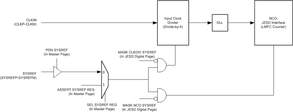
The ADC32RF8x uses SYSREF information to reset the clock divider, the NCO phase, and the LMFC counter of the JESD interface. The device provides flexibility to provide SYSREF information either from dedicated pins or through SPI register bits. As shown in Figure 8-11, SYSREF is asserted by a low-to-high transition on the SYSREF pins or a 0-to-1 change in the ASSERT SYSREF REG bit when using SPI registers.
 Figure 8-11 Using SYSREF to Reset the Clock Divider, the NCO, and the LMFC Counter
The ADC32RF8x samples the SYSREF signal on the input clock rising edge. Required setup and hold time are listed in the Section 6.10 table. The input clock divider gets reset each time that SYSREF is asserted, whereas the NCO phase and the LMFC counter of the JESD interface are reset on each SYSREF assertion after disregarding the first two assertions, as shown in Table 8-1.
| SYSREF ASSERTION INDEX | ACTION | ||
|---|---|---|---|
| INPUT CLOCK DIVIDER | NCO PHASE | LMFC COUNTER | |
| 1 | Gets reset | Does not get reset | Does not get reset |
| 2 | Gets reset | Does not get reset | Does not get reset |
| 3 | Gets reset | Gets reset | Gets reset |
| 4 and onwards | Gets reset | Gets reset | Gets reset |
The SYSREF use-cases can be classified broadly into two categories:
- SYSREF is applied as aperiodic multi-shot pulses.
Figure 8-12 shows a case when only a counted number of pulses are applied as SYSREF to the ADC.
Alternatively, the SYSREF buffer can be powered down with the PDN SYSREF bit.Figure 8-12 SYSREF Used as Aperiodic, Finite Number of PulsesAfter the first SYSREF pulse is applied, allow the DLL in the clock path to settle by waiting for the tDLL time (> 40 µs) before applying the second pulse. During this time, mask the SYSREF going to the input clock divider by setting the MASK CLKDIV SYSREF bit so that the divider output phase remains stable. The NCO phase and LMFC counter are reset on the third SYSREF pulse. After the third SYSREF pulse, the SYSREF going to the NCO and JESD block can be disabled by setting the MASK NCO SYSREF bit to avoid any unwanted resets.
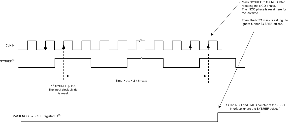
- SYSREF is applied as a periodic pulse.
Figure 8-13 shows how SYSREF can be applied as a continuous periodic waveform.
 tSYSREF is a period of the SYSREF waveform.Alternatively, the SYSREF buffer can be powered down using the PDN SYSREF bit.Figure 8-13 SYSREF Used as a Periodic Waveform
After applying the SYSREF signal, DLL must be allowed to lock, and the NCO phase and LMFC counter must be allowed to reset by waiting for at least the tDLL (40 µs) + 2 × tSYSREF time. Then, the SYSREF going to the NCO and JESD can be masked by setting the MASK NCO SYSREF register bit.