ZHCSEA6B September 2015 – April 2016 ADS1257
PRODUCTION DATA.
- 1 特性
- 2 应用
- 3 说明
- 4 修订历史记录
- 5 Device Comparison Table
- 6 Pin Configuration and Functions
-
7 Specifications
- 7.1 Absolute Maximum Ratings
- 7.2 ESD Ratings
- 7.3 Recommended Operating Conditions
- 7.4 Thermal Information
- 7.5 Electrical Characteristics
- 7.6 Serial Interface Timing Requirements
- 7.7 Serial Interface Switching Characteristics
- 7.8 RESET and SYNC/PWDN Timing Requirements
- 7.9 SCLK Reset Timing Requirements
- 7.10 DRDY Update Timing Characteristics
- 7.11 Typical Characteristics
- 8 Parameter Measurement Information
-
9 Detailed Description
- 9.1 Overview
- 9.2 Functional Block Diagram
- 9.3
Feature Description
- 9.3.1 Input Multiplexer
- 9.3.2 Analog Input Buffer
- 9.3.3 Programmable Gain Amplifier (PGA)
- 9.3.4 Modulator Input Circuitry
- 9.3.5 Voltage Reference Inputs (REFP, REFN)
- 9.3.6 Clock Input (CLKIN)
- 9.3.7 Clock Output (D0/CLKOUT)
- 9.3.8 General-Purpose Digital I/O (D0, D1)
- 9.3.9 Open- and Short-Circuit Sensor Detection
- 9.3.10 Digital Filter
- 9.4 Device Functional Modes
- 9.5
Programming
- 9.5.1 Serial Interface
- 9.5.2 Data Format
- 9.5.3
Command Definitions
- 9.5.3.1 WAKEUP/NOP: Complete Synchronization or Exit Standby Mode
- 9.5.3.2 RDATA: Read Data
- 9.5.3.3 RDATAC: Read Data Continuous
- 9.5.3.4 SDATAC: Stop Read Data Continuous
- 9.5.3.5 RREG: Read from Registers
- 9.5.3.6 WREG: Write to Register
- 9.5.3.7 SELFCAL: Self-Offset and Self-Gain Calibration
- 9.5.3.8 SELFOCAL: Self Offset Calibration
- 9.5.3.9 SELFGCAL: Self Gain Calibration
- 9.5.3.10 SYSOCAL: System Offset Calibration
- 9.5.3.11 SYSGCAL: System Gain Calibration
- 9.5.3.12 STANDBY: Standby Mode / Single-shot Mode
- 9.5.3.13 RESET: Reset Registers to Default Values
- 9.5.3.14 SYNC: Synchronize the Analog-to-Digital Conversion
- 9.6
Register Map
- 9.6.1 STATUS: Status Register (address = 00h) [reset = x1h]
- 9.6.2 MUX : Input Multiplexer Control Register (address = 01h) [reset = 01h]
- 9.6.3 ADCON: ADC Control Register (address = 02h) [reset = 20h]
- 9.6.4 DRATE: ADC Data Rate Register (address = 03h) [reset = F0h]
- 9.6.5 IO: GPIO Control Register (address = 04h) [reset = E0h]
- 9.6.6 OFC0: Offset Calibration Register 0 (address = 05h) [reset = depends on calibration results]
- 9.6.7 OFC1: Offset Calibration Register 1 (address = 06h) [reset = depends on calibration results]
- 9.6.8 OFC2: Offset Calibration Register 2 (address = 07h) [reset = depends on calibration results]
- 9.6.9 FSC0: Full-Scale Calibration Register 0 (address = 08h) [reset = depends on calibration results]
- 9.6.10 FSC1: Full-Scale Calibration Register 1 (address = 09h) [reset = depends on calibration results]
- 9.6.11 FSC2: Full-Scale Calibration Register 2 (address = 0Ah) [reset = depends on calibration results]
- 10Applications and Implementation
- 11Power Supply Recommendations
- 12Layout
- 13器件和文档支持
- 14机械、封装和可订购信息
9 Detailed Description
9.1 Overview
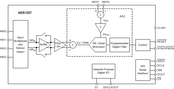
The ADS1257 is a very low-noise ADC that supports four analog inputs and offers two general-purpose digital I/Os. The Functional Block Diagram shows a block diagram of the ADS1257. The input multiplexer selects the ADC input pin connection. Selectable current sources within the input multiplexer check for open- or short-circuit conditions on the external sensor. A selectable input buffer greatly reduces the input circuitry loading by providing up to 80 MΩ of impedance. A low-noise PGA provides gains of 1 V/V, 2 V/V, 4 V/V, 8 V/V, 16 V/V, 32 V/V, or 64 V/V. The ADS1257 is comprised of a fourth-order, delta-sigma modulator followed by a programmable digital filter.
The modulator measures the amplified differential input signal, VIN · Gain = (V(AINP) – V(AINN)) · Gain, against the differential reference, VREF = V(REFP) − V(REFN). The ADC requires an external reference voltage to operate. The differential reference is scaled internally by a factor of two so that the full-scale input range is ±2 · VREF / Gain.
The digital filter receives the modulator signal and provides a low-noise digital output. The data rate of the filter is programmable from 2.5 SPS to 30 kSPS, and allows tradeoffs between resolution and speed.
Communication is over an SPI-compatible serial interface with a set of commands providing control of the ADS1257. The configuration registers store the various settings for the input multiplexer, sensor-detect current sources, input buffer enable, PGA gain setting, output data rate, and more. The ADC requires an external clock source to operate. General-purpose digital I/Os provide static read and write control of up to two pins. The D0 pin is also used to supply a programmable clock output.
9.2 Functional Block Diagram
9.3 Feature Description
9.3.1 Input Multiplexer
Figure 23 shows a simplified diagram of the input multiplexer. Select any pin as the positive input (AINP) and any pin as the negative input (AINN). Pin selection is controlled by the MUX register.
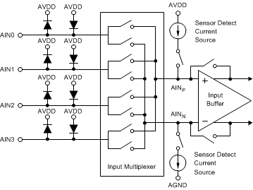 Figure 23. Simplified Diagram of the Input Multiplexer
The ADS1257 offers four analog inputs that can be configured as two independent differential inputs, three single-ended inputs, or a combination of differential and single-ended inputs.
In general, there are no restrictions on input-pin selection. However, follow these recommendations for optimal performance:
- Preferably, use adjacent inputs for differential measurements. For example, use AIN0 and AIN1.
- Leave any unused analog inputs floating, or connect them to AVDD in order to minimize the input-pin leakage current.
ESD diodes protect the analog inputs. To keep these diodes from turning on, voltages on the input pins must not go below AGND by more than 100 mV, and likewise, must not exceed AVDD by more than 100 mV: −100 mV < (V(AINx)) < AVDD + 100 mV.
9.3.2 Analog Input Buffer
To increase the input impedance presented by the ADS1257, enable the low-drift, chopper-stabilized buffer using the BUFEN bit in the STATUS register. As shown in Figure 24, the input impedance with the buffer enabled is modeled by a resistor. Table 5 lists the values of Zeff for the different data-rate settings. The input impedance scales inversely with the frequency of CLKIN. For example, if f(CLKIN) is reduced by half to 3.84 MHz, Zeff for a data-rate setting of 50 SPS (actual data rate of 25 SPS) doubles from 80 MΩ to 160 MΩ.s
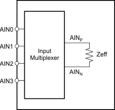 Figure 24. Effective Impedance with Buffer On
Table 5. Input Impedance with Buffer On(1)
| DATA RATE (SPS) |
Zeff (MΩ) |
|---|---|
| ≤ 50 | 80 |
| 60 | 40 |
| 100 | 40 |
| 500 | 40 |
| 1,000 | 20 |
| 2,000 | 10 |
| 3,750 | 10 |
| 7,500 | 10 |
| 15,000 | 10 |
| 30,000 | 10 |
NOTE
With the buffer enabled, the voltage on the analog inputs with respect to ground (listed in the Recommended Operating Conditions as Absolute Input Voltage) must remain between AGND and AVDD − 2.0 V. Exceeding this range reduces performance; in particular, the linearity of the ADS1257. This same voltage range, AGND to AVDD − 2.0 V, applies to the reference inputs when performing a self-gain calibration with the buffer enabled.
9.3.3 Programmable Gain Amplifier (PGA)
The ADS1257 is a very high resolution converter. To further complement converter performance, the low-noise PGA increases the ADC resolution when measuring smaller input signals. For the best resolution, set the PGA to the highest possible gain setting. The gain setting depends on the largest input signal to be measured. The ADS1257 full-scale input voltage equals ±2 · VREF / Gain. Table 6 shows the full-scale input voltage for the different PGA gain settings for VREF = 2.5 V. For example, if the largest signal to be measured is 1.0 V, the optimum PGA gain setting is 4 V/V, producing a full-scale input voltage of 4 V with no ADC overrange.
Table 6. Full-Scale Input Voltage vs PGA Setting
| PGA GAIN SETTING | FULL-SCALE INPUT VOLTAGE VIN (1)
(VREF = 2.5 V) |
|---|---|
| 1 | ±5 V |
| 2 | ±2.5 V |
| 4 | ±1.25 V |
| 8 | ±0.625 V |
| 16 | ±312.5 mV |
| 32 | ±156.25 mV |
| 64 | ±78.125 mV |
The PGA is controlled by the ADCON register. Recalibrate the ADC after changing the PGA gain setting. The time required for self-calibration depends on the PGA gain setting; see the Calibration section for more details. The analog current and input impedance (when the buffer is disabled) vary as a function of the PGA gain setting.
9.3.4 Modulator Input Circuitry
The ADS1257 modulator measures the input signal using internal capacitors that are continuously charged and discharged. Figure 25 shows a simplified schematic of the ADS1257 input circuitry with the input buffer disabled. The on and off timing of the S1 and S2 switches are shown in Figure 26. The S1 switch closes during the input sampling phase. With S1 closed, CA1 charges to V(AINP), CA2 charges to V(AINN), and CB charges to
(V(AINP) – V(AINN)). For the discharge phase, S1 opens first and then S2 closes. CA1 and CA2 discharge to approximately AVDD / 2 and CB discharges to 0 V. This two-phase sample and discharge cycle repeats with a period of tSAMPLE. This time is a function of the PGA gain setting as shown in Table 7 along with the values of capacitors CA1 = CA2 = CA and CB.
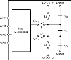 Figure 25. Simplified Input Structure with Buffer Off
 Figure 26. S1 and S2 Switch Timing for Figure 25
Table 7. Input Sampling Time (tSAMPLE), CA, and CB vs PGA Gain
| PGA GAIN SETTING | tSAMPLE(1) | CA | CB |
|---|---|---|---|
| 1 | f(CLKIN) / 4 (521 ns) | 2.1 pF | 2.4 pF |
| 2 | f(CLKIN) / 4 (521 ns) | 4.2 pF | 4.9 pF |
| 4 | f(CLKIN) / 4 (521 ns) | 8.3 pF | 9.7 pF |
| 8 | f(CLKIN) / 4 (521 ns) | 17 pF | 19 pF |
| 16 | f(CLKIN) / 4 (521 ns) | 33 pF | 39 pF |
| 32 | f(CLKIN) / 2 (260 ns) | 33 pF | 39 pF |
| 64 | f(CLKIN) / 2 (260 ns) | 33 pF | 39 pF |
The charging of the input capacitors draws a transient current from the sensor driving the ADS1257 inputs. The average value of this current is used to calculate an effective impedance Zeff, where Zeff = VIN / IAVERAGE. Figure 27 shows the input circuitry with the capacitors and switches of Figure 25 replaced by their effective impedances. These impedances scale inversely with the CLKIN frequency. For example, if f(CLKIN) is reduced by a factor of two, the impedances double. The impedance also changes with the PGA gain setting. Table 8 lists the effective impedances with the buffer off for f(CLKIN) = 7.68 MHz.
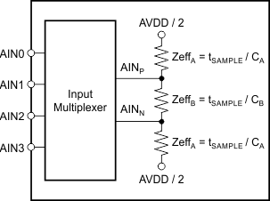 Figure 27. Analog Input Effective Impedances with Buffer Off
Table 8. Analog Input Impedances with Buffer Off(1)
| PGA GAIN SETTING | ZeffA
(kΩ) |
ZeffB
(kΩ) |
|---|---|---|
| 1 | 260 | 220 |
| 2 | 130 | 110 |
| 4 | 65 | 55 |
| 8 | 33 | 28 |
| 16 | 16 | 14 |
| 32 | 8 | 7 |
| 64 | 8 | 7 |
9.3.5 Voltage Reference Inputs (REFP, REFN)
The ADC requires a reference voltage for operation. The reference voltage for the ADS1257 is the differential voltage between REFP and REFN: VREF = V(REFP) − V(REFN). The reference inputs use a structure similar to that of the analog inputs with the circuitry on the reference inputs of Figure 28. The load presented by the switched capacitor is modeled with an effective impedance (Zeff) of 18.5 kΩ for f(CLKIN) = 7.68 MHz. The temperature coefficient of the effective impedance of the voltage reference inputs is approximately 35 ppm/°C.
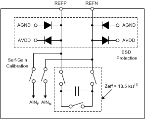
ESD diodes protect the reference inputs. To keep these diodes from turning on, the voltages on the reference pins must not go below AGND by more than 100 mV, and must not exceed AVDD by 100 mV:
AGND − 100 mV < (V(REFP) or V(REFN)) < AVDD + 100 mV
During self gain calibration, all the switches in the input multiplexer are opened, REFN is internally connected to AINN, and REFP is connected to AINP. The input buffer can be disabled or enabled during calibration. When the buffer is disabled, the reference pins drive the circuitry shown in Figure 25 during self gain calibration, resulting in increased loading. To prevent this additional loading from introducing gain errors, the circuitry driving the reference pins must have adequate drive capability. When the buffer is enabled, the loading on the reference pins is much less. However, the buffer limits the allowable voltage range on REFP and REFN during self- or self gain calibration because the reference pins must remain within the specified input range of the buffer in order to establish proper gain calibration.
A high-quality reference voltage capable of driving the switched capacitor load presented by the ADS1257 is essential for achieving the best performance. Noise and drift on the reference degrade overall system performance. Take special care with the circuitry generating the reference voltages and their layout when operating with low-noise settings (that is, with low data rates) in order to prevent the voltage reference from limiting performance.
See the External Reference section for more details.
9.3.6 Clock Input (CLKIN)
The master clock for the ADS1257 must be applied to the CLKIN pin. Keep the external clock signal clean and free of overshoot. Overshoot and glitches on the clock degrade overall performance. See the Recommended Operating Conditions section for the recommended master clock frequency range. Some of the timing requirements, as well as the output data rate, scale directly with the CLKIN frequency.
9.3.7 Clock Output (D0/CLKOUT)
Use the clock output pin (D0/CLKOUT) to clock another device, such as another ADS1257 or a microcontroller. This clock operates at frequencies of f(CLKIN), f(CLKIN) / 2, or f(CLKIN) / 4 and is configured by setting the CLK[1:0] bits in the ADCON register. If the output clock is enabled while driving an external load, the digital power consumption increases. Standby mode does not affect the clock output status. That is, if standby is enabled, the clock output continues to run during standby mode. If not needed, disable the clock output function by writing to the CLK bits in the ADCON register after power-up or reset.
9.3.8 General-Purpose Digital I/O (D0, D1)
The ADS1257 offers two pins dedicated for general-purpose digital I/Os. All of the digital I/O pins can be individually configured as either inputs or outputs through the IO register. The DIR bits of the IO register define whether each pin is an input or output, and the DIO bits control the status of the pins. Reading back the DIO bits shows the state of the digital I/O pins; that is, if configured as inputs or outputs by the DIR bits. When digital I/O pins are configured as inputs, the DIO bits are used to read the state of these pins. When configured as outputs, writing to the DIO bits sets the output value.
During standby and power-down modes, the GPIOs remain active. If configured as outputs, the GPIOs continue to drive the pins. If configured as inputs, the GPIOs must be driven (not left floating) to prevent excess power dissipation.
After power-up or reset, the D1 pin defaults to an input and the D0/CLKOUT pin defaults to the clock output. The CLK[1:0] bits that control the clock output on D0/CLKOUT are only reset after power-up or RESET pin toggle. If the digital I/O pins are not used, either leave them as inputs tied to ground, or configure them as outputs and leave them floating to avoid excess power dissipation.
9.3.9 Open- and Short-Circuit Sensor Detection
The sensor detect current sources (SDCS) provide a means to verify the integrity of the external sensor connected to the ADS1257. When enabled, the SDCS supply a current (ISDC) of approximately 0.5 μA, 2 μA, or 10 μA to the sensor through the input multiplexer. The SDCS bits in the ADCON register enable the SDCS and set the value of ISDC.
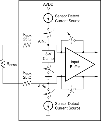
When the SDCS are enabled, the ADS1257 automatically turns on the analog input buffer, regardless of the BUFEN bit setting, in order to prevent the input circuitry from loading the SDCS. AINP must stay below 3 V to be within the absolute input range of the buffer. To help meet this condition, a 3-V clamp starts sinking current from AINP to AGND if AINP exceeds 3 V. Note that this clamp is activated only when the SDCS are enabled.
Figure 29 shows a simplified diagram of the ADS1257 input structure with the external sensor modeled as resistance RSENS between two input pins. When enabled, the SDCS source ISDC to the input pin connected to AINP, and sink ISDC from the input pin connected to AINN. The two 25-Ω series resistors, RMUX, model the ADS1257 internal multiplexer switch on-resistances. The signal measured with the SDCS enabled equals the total IR drop: ISDC × (2RMUX + RSENS). When the sensor is a direct short (that is, RSENS = 0 Ω), there is still a small signal measured by the ADS1257 when the SDCS are enabled: ISDC · 2RMUX.
9.3.10 Digital Filter
The programmable low-pass digital filter receives the modulator output and produces a high-resolution digital output. By adjusting the amount of filtering, tradeoffs can be made between resolution and data rate: filter more for higher resolution, or filter less for higher data rate. The filter is comprised of two sections, a fixed filter followed by a programmable filter. Figure 30 shows the block diagram of the analog modulator and digital filter. Data are supplied to the filter from the analog modulator at a rate of f(MOD) = f(CLKIN) / 4. The fixed filter is a fifth-order sinc filter with a decimation value of 64 that outputs data at a rate of f(CLKIN) / 256. The second stage of the filter is a programmable averager (first-order sinc filter) with the number of averages set by the DRATE register. The data rate is a function of the number of averages (Num_Ave) and is given by Equation 2.

 Figure 30. Block Diagram of the Analog Modulator and Digital Filter
Table 9 shows the averaging and corresponding data rate for each of the 16 valid DRATE register settings when f(CLKIN) = 7.68 MHz. The data rate scales directly with the CLKIN frequency. For example, reducing f(CLKIN) from 7.68 MHz to 3.84 MHz reduces the data rate for DR[7:0] = 1111 0000 from 30,000 SPS to 15,000 SPS.
Table 9. Number of Averages and Data Rate for
Each Valid DRATE Register Setting
| DRATE[7:0] | NUMBER OF AVERAGES FOR PROGRAMMABLE FILTER (Num_Ave) |
DATA RATE(1)
(SPS) |
|---|---|---|
| 0000 0011 (03h) | 12,000 | 2.5 |
| 0001 0011 (13h) | 6000 | 5 |
| 0010 0011 (23h) | 3000 | 10 |
| 0011 0011 (33h) | 2000 | 15 |
| 0100 0011 (43h) | 1200 | 25 |
| 0101 0011 (53h) | 1000 | 30 |
| 0110 0011 (63h) | 600 | 50 |
| 0111 0010 (72h) | 500 | 60 |
| 1000 0010 (82h) | 300 | 100 |
| 1001 0010 (92h) | 60 | 500 |
| 1010 0001 (A1h) | 30 | 1000 |
| 1011 0000 (B0h) | 15 | 2000 |
| 1100 0000 (C0h) | 8 | 3750 |
| 1101 0000 (D0h) | 4 | 7500 |
| 1110 0000 (E0h) | 2 | 15,000 |
| 1111 0000 (F0h) | 1 (averager bypassed) | 30,000 |
9.3.10.1 Frequency Response
The low-pass digital filter sets the overall frequency response for the ADS1257. The filter response is the product of the responses of the fixed and programmable filter sections, and is given by Equation 3:

The digital filter attenuates noise on the modulator output, including noise from within the ADS1257 and external noise present on the ADS1257 input signal. Adjusting the filtering by changing the number of averages used in the programmable filter changes the filter bandwidth. With a higher number of averages, bandwidth is reduced, and more noise is attenuated.
The low-pass filter has notches (or zeros) at the data output rate and multiples thereof. At these frequencies, the filter has zero gain. This feature is useful when trying to reject a particular interference signal. For example, to reduce 60-Hz (and harmonic) noise coupling, set the data rate equal to 2.5 SPS, 5 SPS, 10 SPS, 15 SPS, 30 SPS, or 60 SPS. To help illustrate the filter characteristics, Figure 31 and Figure 32 show the responses at the data-rate extremes of 30 kSPS and 2.5 SPS, respectively.
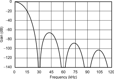 Figure 31. Frequency Response for
Data Rate = 30 kSPS
 Figure 32. Frequency Response for
 Data Rate = 2.5 SPS
Table 10 summarizes the first-notch frequency and −3-dB bandwidth for the different data-rate settings.
Table 10. First Notch Frequency and
-3-dB Filter Bandwidth(1)
| DATA RATE (SPS) |
FIRST NOTCH (Hz) |
-3 dB BANDWIDTH (Hz) |
|---|---|---|
| 2.5 | 2.5 | 1.1 |
| 5 | 5 | 2.21 |
| 10 | 10 | 4.42 |
| 15 | 15 | 6.63 |
| 25 | 25 | 11.1 |
| 30 | 30 | 13.3 |
| 50 | 50 | 22.1 |
| 60 | 60 | 26.5 |
| 100 | 100 | 44.2 |
| 500 | 500 | 221 |
| 1000 | 1000 | 441 |
| 2000 | 2000 | 878 |
| 3750 | 3750 | 1615 |
| 7500 | 7500 | 3003 |
| 15,000 | 15,000 | 4807 |
| 30,000 | 30,000 | 6106 |
The digital filter low-pass characteristic repeats at multiples of the modulator rate of f(MOD) = f(CLKIN) / 4. Figure 33 and Figure 34 show the responses plotted out to 7.68 MHz at the data-rate extremes of 30 kSPS and 2.5 SPS. Notice how the responses near dc, 1.92 MHz, 3.84 MHz, 5.76 MHz, and 7.68 MHz are the same. The digital filter attenuates high-frequency noise on the ADS1257 inputs, except for frequencies where the filter response repeats. External filtering is required to remove high-frequency input noise near these pass-band regions. See the Analog Input Filtering section for more details.
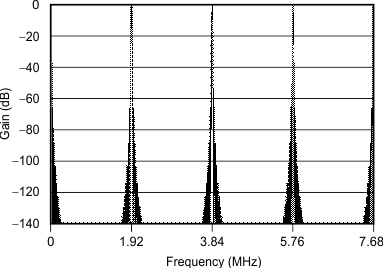 Figure 33. Frequency Response Out to 7.68 MHz
 for Data Rate = 30 kSPS
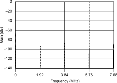 Figure 34. Frequency Response Out to 7.68 MHz
for Data Rate = 2.5 SPS
9.3.10.2 50-Hz and 60-Hz, Line Cycle Rejection
As a result of the proximity of the signal wires to industrial motors and conductors in some applications, coupling of 50-Hz and 60-Hz power-line frequencies can occur. Coupled noise can interfere with the signal voltage leading to inaccurate or unstable conversions. The digital filter rejects power-line interference for data rates of 60 SPS and less. Program the filter to tradeoff data rate and conversion latency versus the desired level of line-cycle rejection. Table 11 summarizes the 50-Hz and 60-Hz line-cycle rejection based on 2% tolerance of power-line frequency to ADC clock frequency.
Table 11. Minimum 50-Hz and 60-Hz, Line-Cycle Rejection
| DATA RATE (SPS) |
MINIMUM DIGITAL-FILTER MAGNITUDE (dB) | |
|---|---|---|
| 50 Hz ±2% | 60 Hz ±2% | |
| 2.5 | –36.2 | –37.4 |
| 5 | –34.4 | –34.6 |
| 10 | –33.9 | –34.0 |
| 15 | — | –33.9 |
| 25 | –33.8 | — |
| 30 | — | –33.8 |
| 50 | –33.8 | — |
| 60 | — | –33.8 |
9.3.10.3 Settling Time
The ADS1257 features a digital filter optimized for fast settling. The Conversion Control and Synchronization section describes the settling time of the ADS1257 for various modes of operation.
9.4 Device Functional Modes
9.4.1 Power-Up
All configuration registers are initialized to default states at power-up. Self-calibration is then performed automatically. For best performance, issue an additional self-calibration with the SELFCAL command or reset the device after the power supplies and voltage reference have settled to their final values.
NOTE
A reset is required after power-up to avoid invalid device operation.
9.4.2 Reset
Three methods are used to reset the ADS1257: the RESET pin, the RESET command, and a special SCLK reset pattern.
- Take the RESET pin low to force a reset. Follow the minimum pulse-width timing specification (t16) before taking the RESET pin high again (see Figure 2).
- Issue the RESET command byte to force a reset (see the RESET section). The RESET command takes effect after all eight bits are shifted into DIN. Afterwards, the reset automatically releases.
- Reset The ADS1257 using a special pattern on SCLK (see Figure 3). Reset occurs on the falling edge of the last SCLK edge in the pattern. CS must be low to perform the SCLK reset pattern. After performing the operation, the reset automatically releases.
After the device resets, the configuration registers are initialized to their default state, except for the CLK[1:0] bits in the ADCON register that control the D0/CLKOUT pin. The CLK[1:0] bits are only initialized to their default state when reset is performed using the RESET pin. Reset also exits from the read-data continuous mode.
After a reset, the device self-calibrates, regardless of the reset method or the state of the ACAL bit before the reset.
9.4.3 Standby Mode
Standby mode shuts down all of the analog circuitry and most of the digital features. To enter standby mode, issue the STANDBY command. To exit standby mode, issue the WAKEUP command. DRDY stays high after exiting standby mode until valid data are ready.
Use standby mode to perform single-shot conversions; see the Settling Time Using Single-Shot Mode section for more information.
If configured as a clock output, the clock signal on the D0/CLKOUT pin continues to run during standby mode.
9.4.4 Power-Down Mode
Hold the SYNC/PWDN pin low for 20 DRDY cycles to activate power-down mode. During power-down mode, all circuitry is disabled including the clock output.
To exit power-down mode, take the SYNC/PWDN pin high. After exiting from power-down mode, 8192 · t(CLKIN) cycles are required before conversions begin.
9.4.5 Conversion Control and Synchronization
Device synchronization is available to control the beginning of the analog-to-digital conversion with an external event, and also to improve settling time after a multiplexer change. Two methods are provided to perform synchronization, the SYNC/PWDN pin or the SYNC command:
- Method 1: Take the SYNC/PWDN pin low and then high, in accordance with timing specifications t16 and t16B. Synchronization occurs when SYNC/PWDN is taken high. No communication is possible on the serial interface while SYNC/PWDN is low. If the SYNC/PWDN pin is held low for 20 DRDY periods, the ADS1257 enters power-down mode.
- Method 2: First, issue the SYNC command. The SYNC command stops the operation of the ADS1257. When ready to synchronize, issue the WAKEUP command. Synchronization occurs on the first rising edge of the master clock after the first SCLK used to shift in the WAKEUP command.
After a synchronization operation, either with the SYNC/PWDN pin or the SYNC command, DRDY stays high until valid data are ready.
The settling time (that is, the time required for a step change on the analog inputs to propagate through the filter) for the different data rates is shown in Table 12 and Figure 35. The following sections highlight the single-cycle settling ability of the filter, and show various ways to control the conversion process.
Table 12. Settling Time Versus Data Rate(1)(2)
| DATA RATE (SPS) |
SETTLING TIME (t18) (ms) |
|---|---|
| 2.5 | 400.18 |
| 5 | 200.18 |
| 10 | 100.18 |
| 15 | 66.84 |
| 25 | 40.18 |
| 30 | 33.51 |
| 50 | 20.18 |
| 60 | 16.84 |
| 100 | 10.18 |
| 500 | 2.18 |
| 1000 | 1.18 |
| 2000 | 0.68 |
| 3750 | 0.44 |
| 7500 | 0.31 |
| 15,000 | 0.25 |
| 30,000 | 0.21 |
9.4.5.1 Settling Time Using Synchronization
The SYNC/PWDN pin and SYNC command allow direct control of conversion timing. Issue a SYNC command or toggle the SYNC/PWDN pin after changing the analog inputs to restart conversions (see the Conversion Control and Synchronization section for more information). The conversion begins when SYNC/PWDN is taken high, thus stopping the current conversion, and restarting the digital filter. As soon as SYNC/PWDN goes low, the DRDY output goes high and remains high during the conversion. DRDY goes low after the settling time (t18, listed for each data rate in Table 12), indicating that data are available. There is no need to ignore or discard data after synchronization. Figure 35 shows the data retrieval sequence following synchronization.
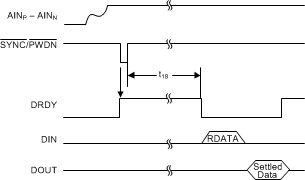 Figure 35. Data Retrieval After Synchronization
9.4.5.2 Settling Time Using Single-Shot Mode
To reduce power consumption in the ADS1257, perform single-shot conversions using the STANDBY command. The sequence for the STANDBY command is shown in Figure 36. Issue the WAKEUP command from standby mode to begin a single-shot conversion. When using single-shot mode, an additional delay is required for the modulator to power up and settle. This delay may require up to 64 modulator clocks (64 · 4 · t(CKLIN)), or 33.3 μs for a 7.68-MHz master clock. Following the settling time (t18 + 256 · t(CLKIN)), DRDY goes low, indicating that the conversion is complete and data can be read using the RDATA command. The ADS1257 settles in a single cycle; there is no need to ignore or discard data. Following the data read cycle, issue another STANDBY command to reduce power consumption. When ready for the next measurement, repeat the cycle starting with another WAKEUP command.
 Figure 36. Single-shot Conversions Using the STANDBY Command
9.4.5.3 Settling Time Using the Input Multiplexer
The most efficient way to cycle through the inputs is to change the multiplexer setting immediately after DRDY goes low. Changing the multiplexer before reading the data allows the ADS1257 to start sampling the new input channel sooner. Figure 37 demonstrates efficient input cycling. There is no need to ignore or discard data while cycling through the channels of the input multiplexer because the ADS1257 data are fully settled when DRDY goes low.
 Figure 37. Cycling the ADS1257 Input Multiplexer
Step 1: When DRDY goes low (indicating that data are ready for retrieval), update the MUX register using the WREG command. For example, setting MUX to 23h selects AINP = AIN2, AINN = AIN3.
Step 2: Restart the conversion process by issuing a SYNC command followed by a WAKEUP command. Follow timing specification t11 between commands.
Step 3: Read the data from the previous conversion using the RDATA command. Repeat this process when DRDY goes low.
Table 13 gives the effective overall throughput (1 / t19) when cycling the input multiplexer. The values for throughput (1 / t19) assume the multiplexer is changed with a 3-byte WREG command and f(SCLK) = f(CLKIN) / 4.
Table 13. Multiplexer Cycling Throughput(1)
| DATA RATE (SPS) |
CYCLING THROUGHPUT (1 / t19) (Hz) |
|---|---|
| 2.5 | 2.5 |
| 5 | 5 |
| 10 | 10 |
| 15 | 15 |
| 25 | 25 |
| 30 | 30 |
| 50 | 50 |
| 60 | 59 |
| 100 | 98 |
| 500 | 456 |
| 1000 | 837 |
| 2000 | 1438 |
| 3750 | 2165 |
| 7500 | 3043 |
| 15,000 | 3817 |
| 30,000 | 4374 |
9.4.5.4 Settling Time while Continuously Converting
After a synchronization, input multiplexer change, or wakeup from standby mode, the ADS1257 continuously converts the analog input. The conversions coincide with the falling edge of DRDY. While continuously converting, the settling time is given by a number of DRDY periods, as shown in Table 14. The DRDY period equals the inverse of the selected data rate.
Table 14. Data Settling Delay Versus Data Rate
| DATA RATE (SPS) |
SETTLING TIME (DRDY PERIODS) |
|---|---|
| 2.5 | 1 |
| 5 | 1 |
| 10 | 1 |
| 15 | 1 |
| 25 | 1 |
| 30 | 1 |
| 50 | 1 |
| 60 | 1 |
| 100 | 1 |
| 500 | 1 |
| 1000 | 1 |
| 2000 | 1 |
| 3750 | 1 |
| 7500 | 2 |
| 15,000 | 3 |
| 30,000 | 5 |
If there is a step change on the input signal while continuously converting, perform a synchronization operation to start a new conversion. Otherwise, the next data represent a combination of the previous and current input signal. Figure 38 shows an example of readback in this situation.
 Figure 38. Step Change on VIN While Continuously Converting for Data Rates ≤ 3750 SPS
9.4.6 Calibration
Minimize offset and gain errors by using the ADS1257 internal calibration features. Figure 39 shows the calibration block diagram. Offset errors are corrected with the offset calibration registers (OFC2, OFC1, and OFC0). Full-scale errors are corrected with the full-scale calibration registers (FSC2, FSC1, and FSC2). Each of these registers are 8-bits with full read and write access. The OFC[2:0] registers and the FSC[2:0] registers both form 24-bit calibration words, referred to as OFC and FSC, respectively.
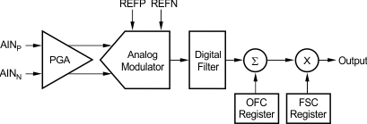 Figure 39. Calibration Block Diagram
The output of the ADS1257 after calibration is shown in Equation 4.

where
- α and β vary with data rate settings shown in Table 15 along with the ideal values (assumes perfect analog performance) for OFC and FSC.
- OFC is a binary twos complement number that can range from −8,388,608 to +8,388,607.
- FSC is unipolar ranging from 0 to 16,777,215.
The ADS1257 supports both self-calibration and system calibration for any PGA gain setting using a set of five commands: SELFOCAL, SELFGCAL, SELFCAL, SYSOCAL, and SYSGCAL. Calibration can be performed at any time; however, in many applications, the ADS1257 drift performance is low enough that a single calibration is all that is needed. DRDY goes high when calibration begins and remains high until settled data are ready. There is no need to discard data after a calibration. For best performance, issue a self-calibration command after power-up when the reference voltage has stabilized. Additionally, performing a reset automatically performs self-calibration. Calibration must be performed whenever the data rate, buffer configuration, or PGA gain changes.
Table 15. Calibration Values for Different Data Rate Settings
| DATA RATE (SPS) |
α | β | IDEAL OFC | IDEAL FSC |
|---|---|---|---|---|
| 2.5 | 5DC000h | 2.7304 | 000000h | 2EE14Ch |
| 5 | 5DC000h | 2.7304 | 000000h | 2EE14Ch |
| 10 | 5DC000h | 2.7304 | 000000h | 2EE14Ch |
| 15 | 3E8000h | 1.8202 | 000000h | 4651F3h |
| 25 | 4B0000h | 2.1843 | 000000h | 3A99A0h |
| 30 | 3E8000h | 1.8202 | 000000h | 4651F3h |
| 50 | 4B0000h | 2.1843 | 000000h | 3A99A0h |
| 60 | 3E8000h | 1.8202 | 000000h | 4651F3h |
| 100 | 4B0000h | 2.1843 | 000000h | 3A99A0h |
| 500 | 3C0000h | 1.7474 | 000000h | 494008h |
| 1000 | 3C0000h | 1.7474 | 000000h | 494008h |
| 2000 | 3C0000h | 1.7474 | 000000h | 494008h |
| 3750 | 400000h | 1.8639 | 000000h | 44AC08h |
| 7500 | 400000h | 1.8639 | 000000h | 44AC08h |
| 15,000 | 400000h | 1.8639 | 000000h | 44AC08h |
| 30,000 | 400000h | 1.8639 | 000000h | 44AC08h |
9.4.6.1 Self-Calibration
Self-calibration corrects internal offset and gain errors. During self-calibration, the appropriate calibration signals are applied internally to the analog inputs. There are three self-calibration commands: SELFOCAL, SELFGCAL, and SELFCAL. As with most of the ADS1257 timings, the calibration time scales directly with f(CLKIN).
9.4.6.1.1 SELFOCAL Command: Self-Offset Calibration
Issuing the SELFOCAL command performs a self-offset calibration. After the command is issued, the analog inputs AINP and AINN are disconnected from the signal source and connected to AVDD / 2. Table 16 lists the self-offset calibration time for the different data-rate settings. Self-offset calibration also updates the OFC register automatically.
Table 16. Self-Offset and System-Offset Calibration Timing(1)
| DATA RATE (SPS) |
SELF OFFSET CALIBRATION AND SYSTEM OFFSET CALIBRATION TIME |
|---|---|
| 2.5 | 800.3 ms |
| 5 | 400.3 ms |
| 10 | 200.3 ms |
| 15 | 133.7 ms |
| 25 | 80.3 ms |
| 30 | 67.0 ms |
| 50 | 40.3 ms |
| 60 | 33.7 ms |
| 100 | 20.3 ms |
| 500 | 4.3 ms |
| 1000 | 2.3 ms |
| 2000 | 1.3 ms |
| 3750 | 853 μs |
| 7500 | 587 μs |
| 15,000 | 453 μs |
| 30,000 | 387 μs |
9.4.6.1.2 SELFGCAL Command: Self-Gain Calibration
Issuing a SELFGCAL command performs a self-gain calibration. After issuing this command, the analog inputs AINP and AINN are disconnected from the signal source and AINP is connected internally to REFP, while AINN is connected to REFN. Self-gain calibration can be used with any PGA gain setting. The ADS1257 has low initial gain error and gain drift, even for the higher PGA gain settings, as shown in the Typical Characteristics section. Using the buffer limits the reference input voltage range during self-gain calibration because the reference is connected to the buffer inputs, and must be within the specified absolute input voltage range. When the voltage on REFP or REFN exceeds the buffer analog input range (AVDD – 2.0 V), the buffer must be turned off during self-gain calibration. Otherwise, use system gain calibration, or write the gain coefficients directly to the FSC register. Table 17 lists the self-gain calibration time for the different data-rate and PGA-gain settings. Self-gain calibration also updates the FSC register automatically.
Table 17. Self Gain Calibration Timing(1)
| DATA RATE (SPS) | PGA GAIN SETTING | ||||
|---|---|---|---|---|---|
| 1 | 2 | 4 | 8 | 16, 32, 64 | |
| 2.5 | 827.0 ms | ||||
| 5 | 413.7 ms | ||||
| 10 | 207.0 ms | ||||
| 15 | 135.3 ms | ||||
| 25 | 83.0 ms | ||||
| 30 | 67.8 ms | ||||
| 50 | 41.7 ms | ||||
| 60 | 34.1 ms | ||||
| 100 | 21.0 ms | ||||
| 500 | 4.5 ms | ||||
| 1000 | 2.4 ms | ||||
| 2000 | 1.4 ms | ||||
| 3750 | 884 | ||||
| 7500 | 617 μs | 617 μs | 617 μs | 617 μs | 751 μs |
| 15,000 | 484 μs | 484 μs | 484 μs | 551 μs | 551 μs |
| 30,000 | 417 μs | 417 μs | 451 μs | 517 μs | 651 μs |
9.4.6.1.3 SELFCAL Command: Self-Offset and Self-Gain Calibration
Issuing the SELFCAL command first performs a self-offset calibration, and then a self-gain calibration. The analog inputs are disconnected from the signal source during self-calibration. When using the input buffer with self-calibration, observe the absolute voltage range of the reference inputs. Table 18 lists the self-calibration time for the different data-rate settings. Self-calibration also updates both the OFC and FSC registers automatically.
Table 18. Self-Calibration Timing(1)
| DATA RATE (SPS) | PGA GAIN SETTING | ||||
|---|---|---|---|---|---|
| 1 | 2 | 4 | 8 | 16, 32, 64 | |
| 2.5 | 1227.2 ms | ||||
| 5 | 613.8 ms | ||||
| 10 | 307.2 ms | ||||
| 15 | 202.1 ms | ||||
| 25 | 123.2 ms | ||||
| 30 | 101.3 ms | ||||
| 50 | 61.8 ms | ||||
| 60 | 50.9 ms | ||||
| 100 | 31.2 ms | ||||
| 500 | 6.6 ms | ||||
| 1000 | 3.6 ms | ||||
| 2000 | 2.0 ms | ||||
| 3750 | 1.3 ms | ||||
| 7500 | 896 μs | 896 μs | 896 μs | 896 μs | 1029 μs |
| 15,000 | 696 μs | 696 μs | 696 μs | 762 μs | 896 μs |
| 30,000 | 596 μs | 596 μs | 692 μs | 696 μs | 892 μs |
9.4.6.2 System Calibration
System calibration corrects both internal and external offset and gain errors using the SYSOCAL and SYSGCAL commands. During system calibration, apply the appropriate calibration signals directly to the inputs.
9.4.6.2.1 SYSOCAL Command: System-Offset Calibration
The SYSOCAL command performs a system-offset calibration. A zero-input differential signal must be supplied. The ADS1257 computes a value that nullifies the offset in the system, and then updates the OFC register.Table 16 shows the time required for system offset calibration for the different data-rate settings. This timing is the same as for the self-offset calibration.
9.4.6.2.2 SYSGCAL Command: System-Gain Calibration
The SYSGCAL command performs a system-gain calibration. A near full-scale input signal to the ADS1257 must be supplied. The ADS1257 computes a value to nullify the gain error in the system, and then automatically updates the FSC register. System-gain calibration corrects inputs that are greater than or equal to 80% of the full-scale input voltage. Do not exceed the full-scale input voltage when using system-gain calibration.
To calibrate with a signal less than full-scale (for example 95% full-scale), follow these steps:
- Apply a near full-scale input signal and configure the registers settings for the appropriate mux inputs, data rate, PGA gain, and buffer state.
- Perform system-gain calibration with the SYSGCAL command and wait for DRDY to go low.
- Read back the calculated FSC value (24-bit word).
- Multiply the FSC value by the ratio of the calibration signal to full-scale voltage (for example, 0.95 for an calibration signal of 95% full-scale).
- Write the result of step 4 into the FSC[2:0] registers.
Table 19 shows the system gain calibration time for the different data-rate settings.
Table 19. System-Gain Calibration Timing(1)
| DATA RATE (SPS) |
SYSTEM GAIN CALIBRATION TIME |
|---|---|
| 2.5 | 800.4 ms |
| 5 | 400.4 ms |
| 10 | 200.4 ms |
| 15 | 133.7 ms |
| 25 | 80.4 ms |
| 30 | 67.0 ms |
| 50 | 40.4 ms |
| 60 | 33.7 ms |
| 100 | 20.4 ms |
| 500 | 4.4 ms |
| 1000 | 2.4 ms |
| 2000 | 1.4 ms |
| 3750 | 884 μs |
| 7500 | 617 μs |
| 15,000 | 484 μs |
| 30,000 | 417 μs |
9.4.6.3 Auto-Calibration
Enable auto-calibration (ACAL bit in STATUS register) in order for the ADS1257 to automatically initiate a self-calibration at the completion of a write command (WREG) that changes the data rate, PGA gain setting, or buffer state.
9.5 Programming
9.5.1 Serial Interface
The SPI-compatible serial interface consists of four signals (CS, SCLK, DIN, and DOUT), and is used to read conversion data, read and write register data, and send ADC control commands. The programmable functions are controlled using a set of configuration registers. Data are written to and read from these registers through the serial interface. See the Serial Interface Timing Requirements section and Figure 1 for additional details on interfacing with the ADS1257.
9.5.1.1 Chip Select (CS)
The chip select (CS) input allows individual selection of a ADS1257 device when multiple devices share the same serial bus. CS must remain low for the duration of the serial communication. When CS is taken high, the serial interface is reset and DOUT enters a high-impedance state. CS can be permanently tied to DGND if not used.
9.5.1.2 Serial Clock (SCLK)
The serial clock (SCLK) features a Schmitt-triggered input, and is used to clock data on the DIN and DOUT pins into and out of (respectively) the ADS1257. Even though the input has hysteresis, keep the SCLK signal as clean as possible to prevent glitches from accidentally shifting data. If SCLK is held low for 32 · DRDY periods, the serial interface resets and the next SCLK pulse starts a new communication cycle. Use this timeout feature to recover communication when a serial interface transmission is interrupted. Apply a special pattern on SCLK to reset the ADC; see the RESET section for more details on this procedure. When the serial interface is idle, hold SCLK low.
9.5.1.3 Data Input (DIN) and Data Output (DOUT)
Use the data input pin (DIN) along with SCLK to send data to the ADS1257. Use the data output pin (DOUT) along with SCLK to read data from the ADS1257. Data on DIN are shifted into the device on the falling edge of SCLK, while data are shifted out on DOUT on the rising edge of SCLK. DOUT is high impedance when not in use in order to allow DIN and DOUT to be connected together, and then driven by a bidirectional driver. Do not issue the RDATAC command while DIN and DOUT are connected together.
9.5.1.4 Data Ready (DRDY)
The DRDY output is a status signal that indicates when a conversion has completed and new data are available to read. DRDY goes low when new conversion data are available, and returns high after all 24 bits are read back using the read data (RDATA) or read data continuous (RDATAC) command. If data are not retrieved, DRDY returns high while new conversion data are updated, as shown in Figure 40 (see the DRDY Update Timing Characteristics section for more information). Do not retrieve data while data are updating; reading data during this period results in invalid data.
 Figure 40. DRDY With No Data Retreival
After changing the PGA gain, data rate, buffer setting, sensor-detect current-source setting, or writing to the OFC or FSC registers, perform a synchronization operation to restart conversions and force DRDY high. DRDY stays high until valid data are ready. If auto-calibration is enabled (by setting the ACAL bit in the STATUS register), DRDY goes low after self-calibration is complete and new data are valid. Exiting standby or power-down mode, or performing a reset or SYNC command also forces DRDY high. DRDY goes low again when valid data are ready.
9.5.2 Data Format
The ADS1257 outputs 24 bits of data in binary twos complement format. The least significant bit (LSB) has a value of (4 · VREF / gain) / 224 V. A positive full-scale input produces an output code of 7FFFFFh, and the negative full-scale input produces an output code of 800000h. The output clips at these codes for signals exceeding full-scale. Table 20 summarizes the ideal output codes for different input signals.
Table 20. Ideal Output Code Versus Input Signal
| INPUT SIGNAL VIN = V(AINP) − V(AINN) |
IDEAL OUTPUT CODE(1) |
|---|---|
| +(2 · VREF / Gain) · (223 – 1) / 223 | 7FFFFFh |
| +(2 · VREF / Gain) / 223 | 000001h |
| 0 | 000000h |
| –(2 · VREF / Gain) / 223 | FFFFFFh |
| ≤ –(2 · VREF / Gain) | 800000h |
9.5.3 Command Definitions
The commands summarized in Table 21 control the operation of the ADS1257. All of the commands are stand-alone except for read data (RDATA) and the the register reads and writes (RREG, WREG) which require a second command byte plus data. Additional command and data bytes may be shifted in without delay after the first command byte. The ORDER bit in the STATUS register sets the order of the bits within the output data. CS must stay low during the entire command sequence.
Table 21. Command Defintions(1)
| COMMAND | DESCRIPTION | 1ST COMMAND BYTE | 2ND COMMAND BYTE | |
|---|---|---|---|---|
| WAKEUP/NOP | Completes SYNC, exits standby mode, and clocks out data | 0000 0000 | (00h) | |
| RDATA | Read data | 0000 0001 | (01h) | |
| RDATAC | Read data continuous | 0000 0011 | (03h) | |
| SDATAC | Stop read data continuous | 0000 1111 | (0Fh) | |
| RREG | Read from REG rrrr | 0001 rrrr | (1xh) | 0000 nnnn |
| WREG | Write to REG rrrr | 0101 rrrr | (5xh) | 0000 nnnn |
| SELFCAL | Offset and gain self-calibration | 1111 0000 | (F0h) | |
| SELFOCAL | Offset self-calibration | 1111 0001 | (F1h) | |
| SELFGCAL | Gain self-calibration | 1111 0010 | (F2h) | |
| SYSOCAL | System offset calibration | 1111 0011 | (F3h) | |
| SYSGCAL | System gain calibration | 1111 0100 | (F4h) | |
| SYNC | Synchronize the analog-to-digital conversion | 1111 1100 | (FCh) | |
| STANDBY | Enter standby mode | 1111 1101 | (FDh) | |
| RESET | Reset to default values | 1111 1110 | (FEh) | |
| WAKEUP/NOP | Completes SYNC, exits standby mode, and clocks out data | 1111 1111 | (FFh) | |
rrrr = starting register address for read or write commands.
9.5.3.1 WAKEUP/NOP: Complete Synchronization or Exit Standby Mode
The WAKEUP and NOP commands are issued by holding DIN high or low, while sending eight SCLKs. The WAKEUP command is used in conjunction with the SYNC and STANDBY commands, and the NOP command is used to clock out data.
9.5.3.2 RDATA: Read Data
Issue the RDATA command after DRDY goes low to read a single conversion result. After all 24 bits are shifted out on DOUT, DRDY goes high. It is not necessary to read back all 24 bits, but DRDY does not return high until new data are updated. See the Serial Interface Timing Requirements for the required delay between the end of the RDATA command and the beginning of data shift on DOUT: t6.
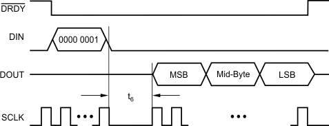 Figure 41. RDATA Command Sequence
9.5.3.3 RDATAC: Read Data Continuous
Issue the RDATAC command after DRDY goes low to enter the read-data-continuous mode. This mode enables the continuous output of new data on each DRDY without the need to issue subsequent read commands. After all 24 bits are read, DRDY goes high. It is not necessary to read back all 24 bits, but DRDY does not return high until new data are updated. This mode is terminated by the stop-read-data-continuous command (SDATAC). Terminate the read-data-continuous mode before reading and writing the device register settings. See the Serial Interface Timing Requirements section for the required t6 delay between the end of the RDATAC command and the beginning of shifting data on DOUT.
 Figure 42. RDATAC Command Sequence
In read-data-continuous mode, shift out data by sending NOP commands. Three NOP commands are required to retrieve all 24 bits of data. The read data continuous mode terminates if input_data equals the SDATAC or RESET command in any of the three bytes on DIN.
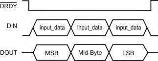 Figure 43. DIN and DOUT Command Sequence During Read Continuous Mode
NOTE
Do not use read-data-continuous mode if DIN and DOUT are connected together, if DRDY is not used, or if reading data cannot be completed before the next DRDY falling edge.
9.5.3.4 SDATAC: Stop Read Data Continuous
The SDATAC command ends read-data-continuous mode and allows the device registers to be read or modified. The SDATAC command must be issued after DRDY goes low and completed before DRDY goes high.
 Figure 44. SDATAC Command Sequence
9.5.3.5 RREG: Read from Registers
Use the RREG command to output the data from up to 11 configuration registers starting at the register address specified as part of the command. The number of registers read is one plus the second byte of the command. If the count exceeds the remaining registers, the addresses wrap back to the beginning. Exit read-data-continuous mode (with the SDATAC command) before issuing a RREG command.
First command byte: 0001 rrrr, where rrrr is the address of the first register to read.
Second command byte: 0000 nnnn, where nnnn is the number of bytes to read – 1. See the Serial Interface Timing Requirements section for the required delay between the end of the RREG command and the beginning of shifting data on DOUT: t6.
 Figure 45. RREG Command Example: Read Two Registers Starting From Register 01h (MUX)
9.5.3.6 WREG: Write to Register
Use the WREG command to write to the configuration registers starting at the register address specified as part of the command. The number of registers that are written is one plus the value of the second byte in the command. If auto-calibration is enabled, writing to the PGA[2:0], DR [7:0] or BUFEN fields starts a self-calibration. Exit read-data-continuous mode (with the SDATAC command) before issuing a WREG command.
First command byte: 0101 rrrr, where rrrr is the address of the first register to be written.
Second command byte: 0000 nnnn, where nnnn is the number of bytes to be written – 1.
Data bytes: one or more data bytes to be written to the device registers.
 Figure 46. WREG Command Example: Write Two Registers Starting From 03h (DRATE)
9.5.3.7 SELFCAL: Self-Offset and Self-Gain Calibration
This command performs both a self-offset and self-gain calibration, as described in the Self-Calibration section. The offset calibration registers (OFC2, OFC1, and OFC0) and full-scale calibration registers (FSC2, FSC1, and FSC0) are updated after this operation. The SELFCAL command must be issued after DRDY goes low. DRDY goes high at the beginning of the calibration. Do not send any additional commands during calibration. DRDY goes low after the calibration completes and settled data are ready.
9.5.3.8 SELFOCAL: Self Offset Calibration
This command performs a self-offset calibration, as described in the Self-Calibration section. The offset calibration registers (OFC2, OFC1, and OFC0) are updated after this operation. The SELFOCAL command must be issued after DRDY goes low. DRDY goes high at the beginning of the calibration. Do not send any additional commands during calibration. DRDY goes low after the calibration completes and settled data are ready.
9.5.3.9 SELFGCAL: Self Gain Calibration
This command performs a self-gain calibration, as described in the Self-Calibration section. The full-scale calibration registers (FSC2, FSC1, and FSC0) are updated after this operation. The SELFGCAL command must be issued after DRDY goes low. DRDY goes high at the beginning of the calibration. Do not send any additional commands during calibration. DRDY goes low after the calibration completes and settled data are ready.
9.5.3.10 SYSOCAL: System Offset Calibration
This command performs a system-offset calibration, as described in the System Calibration section. The offset calibration registers (OFC2, OFC1, and OFC0) are updated after this operation. The SYSOCAL command must be issued after DRDY goes low. DRDY goes high at the beginning of the calibration. Do not send any additional commands during calibration. DRDY goes low after the calibration completes and settled data are ready.
9.5.3.11 SYSGCAL: System Gain Calibration
This command performs a system-gain calibration, as described in the System Calibration section. The full-scale calibration registers (FSC2, FSC1, and FSC0) are updated after this operation. The SYSGCAL command must be issued after DRDY goes low. DRDY goes high at the beginning of the calibration. Do not send any additional commands during calibration. DRDY goes low after the calibration completes and settled data are ready.
9.5.3.12 STANDBY: Standby Mode / Single-shot Mode
The STANDBY command puts the ADS1257 into a low-power standby mode. After issuing the STANDBY command, no more activity on SCLK may occur while CS is low, because SCLK activity interrupts standby mode. SCLK activity does not interrupt standby mode while CS is high. To exit standby mode, issue the WAKEUP command. This command can also be used to perform single conversions (see the Settling Time Using Single-Shot Mode section for more details). The STANDBY command must be issued after DRDY goes low.
 Figure 47. STANDBY Command Sequence
9.5.3.13 RESET: Reset Registers to Default Values
The RESET command returns all configuration registers to their default values, except for the CLK[1:0] bits in the ADCON register. This command also stops read-data-continuous mode. If operating in read-data-continuous mode, issue the RESET command after DRDY goes low.
9.5.3.14 SYNC: Synchronize the Analog-to-Digital Conversion
The SYNC command synchronizes the analog-to-digital conversion. To use the SYNC command, shift in the SYNC command followed by the WAKEUP command. Synchronization occurs on the first CLKIN rising edge after the first SCLK rising edge used to shift in the WAKEUP command. See the Serial Interface Timing Requirements section for the required delay between the end of the SYNC command and the beginning of the WAKEUP command: t11.
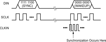 Figure 48. SYNC Command Sequence
9.6 Register Map
The operation of the ADS1257 is controlled through a set of configuration registers. Collectively, the registers contain all the information needed to configure the part, such as data rate, multiplexer settings, PGA gain setting, calibration, and more, and are listed in Table 22.
Table 22. Register Map
| ADDRESS | REGISTER | RESET | BIT 7 | BIT 6 | BIT 5 | BIT 4 | BIT 3 | BIT 2 | BIT 1 | BIT 0 |
|---|---|---|---|---|---|---|---|---|---|---|
| 00h | STATUS | x1h | ID[3:0] | ORDER | ACAL | BUFEN | DRDY | |||
| 01h | MUX | 01h | 0 | 0 | PSEL[1:0] | 0 | 0 | NSEL[1:0] | ||
| 02h | ADCON | 20h | 0 | CLK[1:0] | SDCS[1:0] | PGA[2:0] | ||||
| 03h | DRATE | F0h | DR[7:0] | |||||||
| 04h | IO | E0h | 1 | 1 | DIR1 | DIR0 | 0 | 0 | DIO1 | DIO0 |
| 05h | OFC0 | xxh | OFC[7:0] | |||||||
| 06h | OFC1 | xxh | OFC[15:8] | |||||||
| 07h | OFC2 | xxh | OFC[23:16] | |||||||
| 08h | FSC0 | xxh | FSC[7:0] | |||||||
| 09h | FSC1 | xxh | FSC[15:8] | |||||||
| 0Ah | FSC2 | xxh | FSC[23:16] | |||||||
9.6.1 STATUS: Status Register (address = 00h) [reset = x1h]
| 7 | 6 | 5 | 4 | 3 | 2 | 1 | 0 |
| ID[3:0] | ORDER | ACAL | BUFEN | DRDY | |||
| R-xh | R/W-0h | R/W-0h | R/W-0h | R-1h | |||
| LEGEND: R/W = Read/Write; R = Read only; x = Variable; -n = value after reset |
Table 23. STATUS Register Field Descriptions
| Bit | Field | Type | Reset | Description |
|---|---|---|---|---|
| 7:4 | ID[3:0] | R | xh | Factory programmed identification bits
NOTE: These bits can change without notice. |
| 3 | ORDER | R/W | 0h | Data output bit order
Input data are always shifted in most significant bit first. Output data are always shifted out most significant byte first. The ORDER bit only controls the bit order of the output data within the byte. 0: Most significant bit first (default) 1: Least significant bit first |
| 2 | ACAL | R/W | 0h | Auto-calibration
When auto-calibration is enabled, self-calibration begins at the completion of the WREG command that changes the PGA[2:0], DR [7:0] or BUFEN values. 0: Auto-calibration disabled (default) 1: Auto-calibration enabled |
| 1 | BUFEN | R/W | 0h | Analog input buffer enable
Enables or disables the input buffer. The buffer is automatically enabled when the SDCS are enabled. 0: Buffer disabled (default) 1: Buffer enabled |
| 0 | DRDY | R | 1h | Data ready
This bit duplicates the state of the DRDY pin. |
9.6.2 MUX : Input Multiplexer Control Register (address = 01h) [reset = 01h]
| 7 | 6 | 5 | 4 | 3 | 2 | 1 | 0 |
| 0 | 0 | PSEL[1:0] | 0 | 0 | NSEL[1:0] | ||
| R/W-0h | R/W-0h | R/W-0h | R/W-0h | R/W-0h | R/W-1h | ||
| LEGEND: R/W = Read/Write; R = Read only; x = Variable; -n = value after reset |
Table 24. MUX Register Field Descriptions
| Bit | Field | Type | Reset | Description |
|---|---|---|---|---|
| 7 | 0 | R/W | 0h | Reserved
Always write 0 |
| 6 | 0 | R/W | 0h | Reserved
Always write 0 |
| 5:4 | PSEL[1:0] | R/W | 0h | Positive input channel (AINP) selection
Selects the positive multiplexer input. 00: AIN0 (default)01: AIN1 10: AIN2 11: AIN3 |
| 3 | 0 | R/W | 0h | Reserved
Always write 0 |
| 2 | 0 | R/W | 0h | Reserved
Always write 0 |
| 1:0 | NSEL[1:0] | R/W | 1h | Negative input channel (AINN) selection
Selects the negative multiplexer input. 00: AIN001: AIN1 (default) 10: AIN2 11: AIN3 |
9.6.3 ADCON: ADC Control Register (address = 02h) [reset = 20h]
| 7 | 6 | 5 | 4 | 3 | 2 | 1 | 0 |
| 0 | CLK[1:0] | SDCS[1:0] | PGA[2:0] | ||||
| R-0h | R/W-1h | R/W-0h | R/W-0h | ||||
| LEGEND: R/W = Read/Write; R = Read only; x = Variable; -n = value after reset |
Table 25. ADCON Register Field Descriptions
| Bit | Field | Type | Reset | Description |
|---|---|---|---|---|
| 7 | 0 | R | 0h | Reserved
Always write 0 |
| 6:5 | CLK[1:0] | R/W | 1h | D0/CLKOUT clock output rate setting
When CLKOUT is not used, turn CLKOUT off (00b). These bits can only be reset using the RESET pin. 00: Clock output off01: f(CLKOUT) = f(CLKIN) (default) 10: f(CLKOUT) = f(CLKIN) / 2 11: f(CLKOUT) = f(CLKIN) / 4 |
| 4:3 | SDCS[1:0] | R/W | 0h | Sensor detect current source setting
The sensor detect current sources is activated to verify the integrity of an external sensor supplying a signal to the ADS1257. A shorted sensor produces a very small signal; an open-circuit sensor produces a very large signal. 00: Off (default)01: 0.5 μA 10: 2 μA 11: 10 μA |
| 2:0 | PGA[2:0] | R/W | 0h | PGA gain setting
Selects the PGA gain 000: 1 V/V (default)001: 2 V/V 010: 4 V/V 011: 8 V/V 100: 16 V/V 101: 32 V/V 110: 64 V/V 111: 64 V/V |
9.6.4 DRATE: ADC Data Rate Register (address = 03h) [reset = F0h]
| 7 | 6 | 5 | 4 | 3 | 2 | 1 | 0 |
| DR[7:0] | |||||||
| R/W-F0h | |||||||
| LEGEND: R/W = Read/Write; R = Read only; x = Variable; -n = value after reset |
Table 26. DRATE Register Field Descriptions
| Bit | Field | Type | Reset | Description |
|---|---|---|---|---|
| 7:0 | DR[7:0] | R/W | F0h | Data rate setting(1)
Selects the ADC data rate 0000 0011 (03h): 2.5 SPS0001 0011 (13h): 5 SPS 0010 0011 (23h): 10 SPS 0011 0011 (33h): 15 SPS 0100 0011 (43h): 25 SPS 0101 0011 (53h): 30 SPS 0110 0011 (63h): 50 SPS 0111 0010 (72h): 60 SPS 1000 0010 (82h): 100 SPS 1001 0010 (92h): 500 SPS 1010 0001 (A1h): 1,000 SPS 1011 0000 (B0h): 2,000 SPS 1100 0000 (C0h): 3,750 SPS 1101 0000 (D0h): 7,500 SPS 1110 0000 (E0h): 15,000 SPS 1111 0000 (F0h): 30,000 SPS (default) |
9.6.5 IO: GPIO Control Register (address = 04h) [reset = E0h]
The states of these bits control the operation of the general-purpose digital I/O pins. The ADS1257 has two digital I/O pins: D0/CLKOUT and D1.
| 7 | 6 | 5 | 4 | 3 | 2 | 1 | 0 |
| 1 | 1 | DIR1 | DIR0 | 0 | 0 | DIO1 | DIO0 |
| R/W-1h | R/W-1h | R/W-1h | R/W-0h | R/W-0h | R/W-0h | R/W-0h | R/W-0h |
| LEGEND: R/W = Read/Write; R = Read only; x = Variable; -n = value after reset |
Table 27. IO Register Field Descriptions
| Bit | Field | Type | Reset | Description |
|---|---|---|---|---|
| 7 | 1 | R/W | 1h | Reserved
Always write 1 |
| 6 | 1 | R/W | 1h | Reserved
Always write 1 |
| 5 | DIR1 | R/W | 1h | Digital I/O direction for D1 pin
Configures D1 as a GPIO input or GPIO output 0: D1 is an output 1: D1 is an input (default) |
| 4 | DIR0 | R/W | 0h | Digital I/O direction for D0/CLKOUT pin
0: D0/CLKOUT is a GPIO or clock output (default) 1: D0/CLKOUT is a GPIO input |
| 3 | 0 | R/W | 0h | Reserved
Always write 0 |
| 2 | 0 | R/W | 0h | Reserved
Always write 0 |
| 1 | DIO1 | R/W | 0h | Status of digital I/O pin D1
Reading this bit shows the state of the D1 pin, regardless of the DIR1 bit configuration. When D1 is configured as an output by the DIR1 bit, writing to the this bit sets the output state of D1. When D1 is configured as an input by the DIR1 bit, writing to this bit has no effect. |
| 0 | DIO0 | R/W | 0h | Status of digital I/O pin D0/CLKOUT
When D0/CLKOUT is configured as an input (DIR0 = 1), reading this bit shows the state of the D0/CLKOUT pin. When D0/CLKOUT is configured as an input (DIR0 = 1), writing to this bit has no effect. When D0/CLKOUT is configured as an output (DIR0 = 0) and CLKOUT is disabled (CLK[1:0] = 0), writing to this bit sets the output state of D0/CLKOUT. When D0/CLKOUT is configured as an output (DIR0 = 0) and CLKOUT is enabled (CLK[1:0] ≠ 0), writing to this bit has no effect. |
9.6.6 OFC0: Offset Calibration Register 0 (address = 05h) [reset = depends on calibration results]
| 7 | 6 | 5 | 4 | 3 | 2 | 1 | 0 |
| OFC[7:0] | |||||||
| R/W-xxh | |||||||
| LEGEND: R/W = Read/Write; R = Read only; x = Variable; -n = value after reset |
9.6.7 OFC1: Offset Calibration Register 1 (address = 06h) [reset = depends on calibration results]
| 7 | 6 | 5 | 4 | 3 | 2 | 1 | 0 |
| OFC[15:8] | |||||||
| R/W-xxh | |||||||
| LEGEND: R/W = Read/Write; R = Read only; x = Variable; -n = value after reset |
9.6.8 OFC2: Offset Calibration Register 2 (address = 07h) [reset = depends on calibration results]
| 7 | 6 | 5 | 4 | 3 | 2 | 1 | 0 |
| OFC[23:16] | |||||||
| R/W-xxh | |||||||
| LEGEND: R/W = Read/Write; R = Read only; x = Variable; -n = value after reset |
9.6.9 FSC0: Full-Scale Calibration Register 0 (address = 08h) [reset = depends on calibration results]
| 7 | 6 | 5 | 4 | 3 | 2 | 1 | 0 |
| FSC[7:0] | |||||||
| R/W-xxh | |||||||
| LEGEND: R/W = Read/Write; R = Read only; x = Variable; -n = value after reset |
9.6.10 FSC1: Full-Scale Calibration Register 1 (address = 09h) [reset = depends on calibration results]
| 7 | 6 | 5 | 4 | 3 | 2 | 1 | 0 |
| FSC[15:8] | |||||||
| R/W-xxh | |||||||
| LEGEND: R/W = Read/Write; R = Read only; x = Variable; -n = value after reset |
9.6.11 FSC2: Full-Scale Calibration Register 2 (address = 0Ah) [reset = depends on calibration results]
| 7 | 6 | 5 | 4 | 3 | 2 | 1 | 0 |
| FSC[23:16] | |||||||
| R/W-xxh | |||||||
| LEGEND: R/W = Read/Write; R = Read only; x = Variable; -n = value after reset |