ZHCSCA6B April 2014 – October 2020 ADS4245-EP
PRODUCTION DATA
- 1 特性
- 2 应用
- 3 说明
- 4 Revision History
- 5 Pin Configuration and Functions
-
6 Specifications
- 6.1 Absolute Maximum Ratings
- 6.2 ESD Ratings
- 6.3 Recommended Operating Conditions
- 6.4 Thermal Information
- 6.5 Electrical Characteristics:
- 6.6 Electrical Characteristics: General
- 6.7 Digital Characteristics
- 6.8 Timing Characteristics: LVDS And CMOS Modes
- 6.9 Typical Characteristics:
- 6.10 Typical Characteristics: General
- 6.11 Typical Characteristics: Contour
-
7 Detailed Description
- 7.1 Overview
- 7.2 Functional Block Diagram
- 7.3 Feature Description
- 7.4 Device Functional Modes
- 7.5 Serial Register Map
- 7.6 Description Of Serial Registers
- 8 Application and Implementation
- 9 Power Supply Recommendations
- 10Layout
- 11Device and Documentation Support
7.4.6.4 Parallel Configuration Details
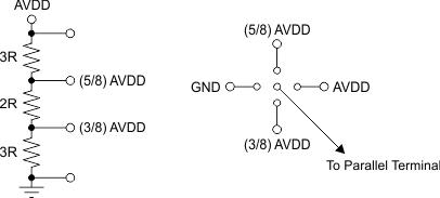
The functions controlled by each parallel terminal are described in Table 7-6, Table 7-7, and Table 7-8. A simple way of configuring the parallel terminals is shown in Figure 7-8.
Table 7-6 SCLK Control Terminal
| VOLTAGE APPLIED ON SCLK | DESCRIPTION |
|---|---|
| Low | Low-speed mode is disabled |
| High | Low-speed mode is enabled(1) |
(1) Low-speed mode is enabled in the ADS4222/42 by default.
Table 7-7 SEN Control Terminal
| VOLTAGE APPLIED ON SEN | DESCRIPTION |
|---|---|
| 0 (+50mV/0mV) | Twos complement and parallel CMOS output |
| (3/8) AVDD (±50mV) | Offset binary and parallel CMOS output |
| (5/8) 2AVDD (±50mV) | Offset binary and DDR LVDS output |
| AVDD (0mV/–50mV) | Twos complement and DDR LVDS output |
Table 7-8 CTRL1, CTRL2, And CTRL3 Terminals
| CTRL1 | CTRL2 | CTRL3 | DESCRIPTION |
|---|---|---|---|
| Low | Low | Low | Normal operation |
| Low | Low | High | Not available |
| Low | High | Low | Not available |
| Low | High | High | Not available |
| High | Low | Low | Global power-down |
| High | Low | High | Channel A standby, channel B is active |
| High | High | Low | Not available |
| High | High | High | MUX mode of operation, channel A and B data are multiplexed and output on the DB[13:0] terminals. |
 Figure 7-8 Simple Scheme To Configure The Parallel Terminals