ZHCSDS3C May 2015 – April 2018 ADS52J90
PRODUCTION DATA.
- 1 特性
- 2 应用
- 3 说明
- 4 修订历史记录
- 5 说明 (续)
- 6 Pin Configuration and Functions
-
7 Specifications
- 7.1 Absolute Maximum Ratings
- 7.2 ESD Ratings
- 7.3 Recommended Operating Conditions
- 7.4 Thermal Information
- 7.5 Electrical Characteristics
- 7.6 Digital Characteristics
- 7.7 Timing Requirements: Signal Chain
- 7.8 Timing Requirements: JESD Interface
- 7.9 Timing Requirements: Serial Interface
- 7.10 Typical Characteristics
- 7.11 Typical Characteristics: JESD Interface
- 7.12 Typical Characteristics: Contour Plots
-
8 Detailed Description
- 8.1 Overview
- 8.2 Functional Block Diagrams
- 8.3
Feature Description
- 8.3.1 Connection of the External Inputs to the Input Pins
- 8.3.2 Input Multiplexer and Sampler
- 8.3.3 Analog-to-Digital Converter (ADC)
- 8.3.4 Device Synchronization Using TX_TRIG
- 8.3.5 Digital Processing
- 8.3.6 Data Formatting
- 8.3.7 Serializer and LVDS Interface
- 8.3.8 LVDS Buffers
- 8.3.9 JESD204B Interface
- 8.3.10 Interfacing SYNC~ and SYSREF Between the FPGA and ADCs
- 8.3.11 Clock Input
- 8.3.12 Analog Input and Driving Circuit
- 8.4 Device Functional Modes
- 8.5 Programming
- 9 Application and Implementation
- 10Power Supply Recommendations
- 11Layout
-
12Register Map
- 12.1
ADC Registers
- 12.1.1
Description of Registers
- 12.1.1.1 Register 0h (address = 0h)
- 12.1.1.2 Register 1h (address = 1h)
- 12.1.1.3 Register 2h (address = 2h)
- 12.1.1.4 Register 3h (address = 3h)
- 12.1.1.5 Register 4h (address = 4h)
- 12.1.1.6 Register 5h (address = 5h)
- 12.1.1.7 Register 7h (address = 7h)
- 12.1.1.8 Register 8h (address = 8h)
- 12.1.1.9 Register Ah (address = Ah)
- 12.1.1.10 Register Bh (address = Bh)
- 12.1.1.11 Register Dh (address = Dh)
- 12.1.1.12 Register Eh (address = Eh)
- 12.1.1.13 Register Fh (address = Fh)
- 12.1.1.14 Register 10h (address = 10h)
- 12.1.1.15 Register 11h (address = 11h)
- 12.1.1.16 Register 12h (address = 12h)
- 12.1.1.17 Register 13h (address = 13h)
- 12.1.1.18 Register 14h (address = 14h)
- 12.1.1.19 Register 15h (address = 15h)
- 12.1.1.20 Register 17h (address = 17h)
- 12.1.1.21 Register 18h (address = 18h)
- 12.1.1.22 Register 19h (address = 19h)
- 12.1.1.23 Register 1Ah (address = 1Ah)
- 12.1.1.24 Register 1Bh (address = 1Bh)
- 12.1.1.25 Register 1Ch (address = 1Ch)
- 12.1.1.26 Register 1Dh (address = 1Dh)
- 12.1.1.27 Register 1Eh (address = 1Eh)
- 12.1.1.28 Register 1Fh (address = 1Fh)
- 12.1.1.29 Register 20h (address = 20h)
- 12.1.1.30 Register 21h (offset = 21h)
- 12.1.1.31 Register 23h (register = 23h)
- 12.1.1.32 Register 24h (address = 24h)
- 12.1.1.33 Register 25h (address = 25h)
- 12.1.1.34 Register 26h (address = 26h)
- 12.1.1.35 Register 27h (address = 27h)
- 12.1.1.36 Register 28h (address = 28h)
- 12.1.1.37 Register 29h (address = 29h)
- 12.1.1.38 Register 2Ah (address = 2Ah)
- 12.1.1.39 Register 2Bh (address = 2Bh)
- 12.1.1.40 Register 2Ch (address = 2Ch)
- 12.1.1.41 Register 2Dh (address = 2Dh)
- 12.1.1.42 Register 2Fh (address = 2Fh)
- 12.1.1.43 Register 30h (address = 30h)
- 12.1.1.44 Register 31h (address = 31h)
- 12.1.1.45 Register 32h (address = 32h)
- 12.1.1.46 Register 33h (address = 33h)
- 12.1.1.47 Register 34h (address = 34h)
- 12.1.1.48 Register 35h (address = 35h)
- 12.1.1.49 Register 36h (address = 36h)
- 12.1.1.50 Register 37h (address = 37h)
- 12.1.1.51 Register 38h (address = 38h)
- 12.1.1.52 Register 39h (address = 39h)
- 12.1.1.53 Register 3Bh (address = 3Bh)
- 12.1.1.54 Register 3Ch (address = 3Ch)
- 12.1.1.55 Register 43h (address = 43h)
- 12.1.1
Description of Registers
- 12.2
JESD Serial Interface Registers
- 12.2.1
Description of JESD Serial Interface Registers
- 12.2.1.1 Register 70 (address = 46h)
- 12.2.1.2 Register 73 (address = 49h)
- 12.2.1.3 Register 74 (address = 4Ah)
- 12.2.1.4 Register 75 (address = 4Bh)
- 12.2.1.5 Register 77 (address = 4Dh)
- 12.2.1.6 Register 80 (address = 50h)
- 12.2.1.7 Register 81 (address = 51h)
- 12.2.1.8 Register 82 (address = 52h)
- 12.2.1.9 Register 83 (address = 53h)
- 12.2.1.10 Register 85 (address = 55h)
- 12.2.1.11 Register 115 (address = 73h)
- 12.2.1.12 Register 116 (address = 74h)
- 12.2.1.13 Register 117 (address = 75h)
- 12.2.1.14 Register 118 (address = 76h)
- 12.2.1.15 Register 119 (address = 77h)
- 12.2.1.16 Register 120 (address = 78h)
- 12.2.1.17 Register 134 (address = 86h)
- 12.2.1.18 Register 135 (address = 87h)
- 12.2.1.19 Register 136 (address = 88h)
- 12.2.1.20 Register 137 (address = 89h)
- 12.2.1.21 Register 138 (address = 8Ah)
- 12.2.1
Description of JESD Serial Interface Registers
- 12.1
ADC Registers
- 13器件和文档支持
- 14机械、封装和可订购信息
8.3.4 Device Synchronization Using TX_TRIG
The device has multiple PLLs and clock dividers that are used to generate the programmable ADC resolutions and LVDS synchronization factors as well as to synchronize LVDS test patterns.
The TX_TRIG input is used to synchronize clock dividers inside the device. The synchronization achieved using TX_TRIG also enables multiple parallel devices to operate synchronously.
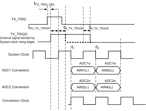
For the 32-input mode, the same ADC alternates between converting two inputs. The TX_TRIG signal provides the mechanism to determine the sampling instants of the odd and even input signals with respect to the system clock, as shown in Figure 60.
 Figure 60. Odd- and Even-Channel Sampling Instant Definition Mechanism in
32-Input Mode with the TX_TRIG Signal
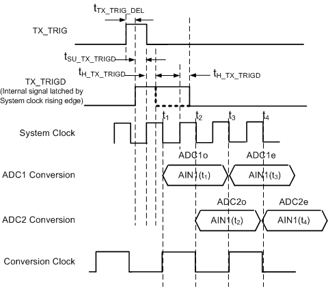
For the 8-input mode, the conversion clock is obtained by dividing the system clock by 2. The phase of the division is again determined by the TX_TRIG signal, as shown in Figure 61.
 Figure 61. Conversion Clock Deriving Mechanism from Division of the Sampling Clock in 8-Input Mode
Applying a pulse on TX_TRIG is a mandatory part of the power-up and initialization sequence; see the Power Sequencing and Initialization section.
In case a TX_TRIG is not applied, the device can possibly behave in an unexpected manner. The identified cases are shown in Table 6.
Table 6. Device Behavior Cases: TX_TRIG is Not Applied
| SCENARIO | ISSUE | INPUT MODE WHERE ISSUE OCCURS
(8-, 16-, 32-Channel Input Modes) |
|---|---|---|
| Multiple devices operating in parallel | Frame clock across devices is not synchronized | 8- and 32-channel input modes |
| LVDS patterns across devices are not synchronized | 8-, 16-, and 32-channel input modes | |
| Serialization factor different from ADC resolution | Framing of data words within a frame clock is not defined | 8- and 32-channel input modes |
The TX_TRIG pulse resets the phase of the test pattern generator, the odd and even sampling phase selection, and the phase of the frame clock. As a result of this phase reset operation, the ADC data can be corrupted for four to six clocks immediately after applying TX_TRIG. The phase reset from TX_TRIG can be disabled using MASK_TX_TRIG.