ZHCSDS3C May 2015 – April 2018 ADS52J90
PRODUCTION DATA.
- 1 特性
- 2 应用
- 3 说明
- 4 修订历史记录
- 5 说明 (续)
- 6 Pin Configuration and Functions
-
7 Specifications
- 7.1 Absolute Maximum Ratings
- 7.2 ESD Ratings
- 7.3 Recommended Operating Conditions
- 7.4 Thermal Information
- 7.5 Electrical Characteristics
- 7.6 Digital Characteristics
- 7.7 Timing Requirements: Signal Chain
- 7.8 Timing Requirements: JESD Interface
- 7.9 Timing Requirements: Serial Interface
- 7.10 Typical Characteristics
- 7.11 Typical Characteristics: JESD Interface
- 7.12 Typical Characteristics: Contour Plots
-
8 Detailed Description
- 8.1 Overview
- 8.2 Functional Block Diagrams
- 8.3
Feature Description
- 8.3.1 Connection of the External Inputs to the Input Pins
- 8.3.2 Input Multiplexer and Sampler
- 8.3.3 Analog-to-Digital Converter (ADC)
- 8.3.4 Device Synchronization Using TX_TRIG
- 8.3.5 Digital Processing
- 8.3.6 Data Formatting
- 8.3.7 Serializer and LVDS Interface
- 8.3.8 LVDS Buffers
- 8.3.9 JESD204B Interface
- 8.3.10 Interfacing SYNC~ and SYSREF Between the FPGA and ADCs
- 8.3.11 Clock Input
- 8.3.12 Analog Input and Driving Circuit
- 8.4 Device Functional Modes
- 8.5 Programming
- 9 Application and Implementation
- 10Power Supply Recommendations
- 11Layout
-
12Register Map
- 12.1
ADC Registers
- 12.1.1
Description of Registers
- 12.1.1.1 Register 0h (address = 0h)
- 12.1.1.2 Register 1h (address = 1h)
- 12.1.1.3 Register 2h (address = 2h)
- 12.1.1.4 Register 3h (address = 3h)
- 12.1.1.5 Register 4h (address = 4h)
- 12.1.1.6 Register 5h (address = 5h)
- 12.1.1.7 Register 7h (address = 7h)
- 12.1.1.8 Register 8h (address = 8h)
- 12.1.1.9 Register Ah (address = Ah)
- 12.1.1.10 Register Bh (address = Bh)
- 12.1.1.11 Register Dh (address = Dh)
- 12.1.1.12 Register Eh (address = Eh)
- 12.1.1.13 Register Fh (address = Fh)
- 12.1.1.14 Register 10h (address = 10h)
- 12.1.1.15 Register 11h (address = 11h)
- 12.1.1.16 Register 12h (address = 12h)
- 12.1.1.17 Register 13h (address = 13h)
- 12.1.1.18 Register 14h (address = 14h)
- 12.1.1.19 Register 15h (address = 15h)
- 12.1.1.20 Register 17h (address = 17h)
- 12.1.1.21 Register 18h (address = 18h)
- 12.1.1.22 Register 19h (address = 19h)
- 12.1.1.23 Register 1Ah (address = 1Ah)
- 12.1.1.24 Register 1Bh (address = 1Bh)
- 12.1.1.25 Register 1Ch (address = 1Ch)
- 12.1.1.26 Register 1Dh (address = 1Dh)
- 12.1.1.27 Register 1Eh (address = 1Eh)
- 12.1.1.28 Register 1Fh (address = 1Fh)
- 12.1.1.29 Register 20h (address = 20h)
- 12.1.1.30 Register 21h (offset = 21h)
- 12.1.1.31 Register 23h (register = 23h)
- 12.1.1.32 Register 24h (address = 24h)
- 12.1.1.33 Register 25h (address = 25h)
- 12.1.1.34 Register 26h (address = 26h)
- 12.1.1.35 Register 27h (address = 27h)
- 12.1.1.36 Register 28h (address = 28h)
- 12.1.1.37 Register 29h (address = 29h)
- 12.1.1.38 Register 2Ah (address = 2Ah)
- 12.1.1.39 Register 2Bh (address = 2Bh)
- 12.1.1.40 Register 2Ch (address = 2Ch)
- 12.1.1.41 Register 2Dh (address = 2Dh)
- 12.1.1.42 Register 2Fh (address = 2Fh)
- 12.1.1.43 Register 30h (address = 30h)
- 12.1.1.44 Register 31h (address = 31h)
- 12.1.1.45 Register 32h (address = 32h)
- 12.1.1.46 Register 33h (address = 33h)
- 12.1.1.47 Register 34h (address = 34h)
- 12.1.1.48 Register 35h (address = 35h)
- 12.1.1.49 Register 36h (address = 36h)
- 12.1.1.50 Register 37h (address = 37h)
- 12.1.1.51 Register 38h (address = 38h)
- 12.1.1.52 Register 39h (address = 39h)
- 12.1.1.53 Register 3Bh (address = 3Bh)
- 12.1.1.54 Register 3Ch (address = 3Ch)
- 12.1.1.55 Register 43h (address = 43h)
- 12.1.1
Description of Registers
- 12.2
JESD Serial Interface Registers
- 12.2.1
Description of JESD Serial Interface Registers
- 12.2.1.1 Register 70 (address = 46h)
- 12.2.1.2 Register 73 (address = 49h)
- 12.2.1.3 Register 74 (address = 4Ah)
- 12.2.1.4 Register 75 (address = 4Bh)
- 12.2.1.5 Register 77 (address = 4Dh)
- 12.2.1.6 Register 80 (address = 50h)
- 12.2.1.7 Register 81 (address = 51h)
- 12.2.1.8 Register 82 (address = 52h)
- 12.2.1.9 Register 83 (address = 53h)
- 12.2.1.10 Register 85 (address = 55h)
- 12.2.1.11 Register 115 (address = 73h)
- 12.2.1.12 Register 116 (address = 74h)
- 12.2.1.13 Register 117 (address = 75h)
- 12.2.1.14 Register 118 (address = 76h)
- 12.2.1.15 Register 119 (address = 77h)
- 12.2.1.16 Register 120 (address = 78h)
- 12.2.1.17 Register 134 (address = 86h)
- 12.2.1.18 Register 135 (address = 87h)
- 12.2.1.19 Register 136 (address = 88h)
- 12.2.1.20 Register 137 (address = 89h)
- 12.2.1.21 Register 138 (address = 8Ah)
- 12.2.1
Description of JESD Serial Interface Registers
- 12.1
ADC Registers
- 13器件和文档支持
- 14机械、封装和可订购信息
8.3.12.1 Signal Input
The analog input to the device can be either ac- or dc-coupled. In ac-coupling, the input common-mode required for device functionality can be forced with the common-mode voltage, generated internally by the device (that comes at the VCM pin) through a resistor, as shown in Figure 89. The resistor and capacitor values used for coupling determines the high-pass filter corner of the input circuit; thus, these values are chosen with the frequency of interest in mind.
 Figure 89. AC Coupling
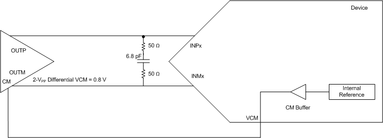
When dc-coupling the analog input, the output common-mode voltage of the driver can be set using the VCM output pin as a reference, as shown in Figure 90.
 Figure 90. DC Coupling
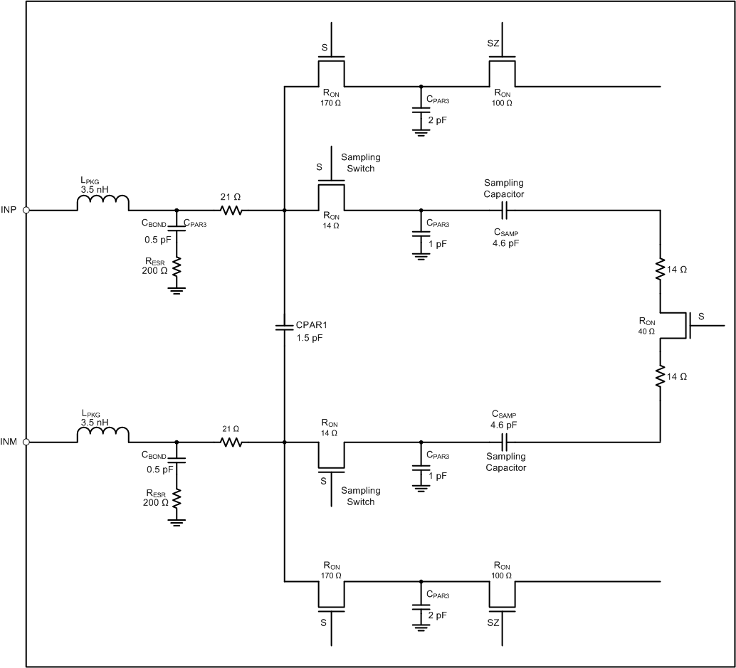
Each input interfaces to two sets of identical sampling circuits. The electrical model of the load that each of the sampling networks present is illustrated in Figure 91. For the sake of simplification, the MOS switches can be considered as ideal switches.
As illustrated in Figure 57, Figure 58, and Figure 59, the scheme of connecting each input sampling circuit to the input pins differs across the three input modes. The time-dependent loading of the input pins therefore is different across the three input modes, and can be determined by referring to Figure 57, Figure 58, Figure 59, and Figure 91.
 Figure 91. Analog Input Sampling Network