SLAS611C October 2009 – January 2016 ADS5400
PRODUCTION DATA.
- 1 Features
- 2 Applications
- 3 Description
- 4 Revision History
- 5 Pin Configuration and Functions
- 6 Specifications
-
7 Detailed Description
- 7.1 Overview
- 7.2 Functional Block Diagram
- 7.3 Feature Description
- 7.4 Device Functional Modes
- 7.5 Programming
- 7.6 Register Maps
- 8 Application and Implementation
- 9 Power Supply Recommendations
- 10Layout
- 11Device and Documentation Support
- 12Mechanical, Packaging, and Orderable Information
封装选项
机械数据 (封装 | 引脚)
- PZP|100
散热焊盘机械数据 (封装 | 引脚)
- PZP|100
订购信息
7 Detailed Description
7.1 Overview
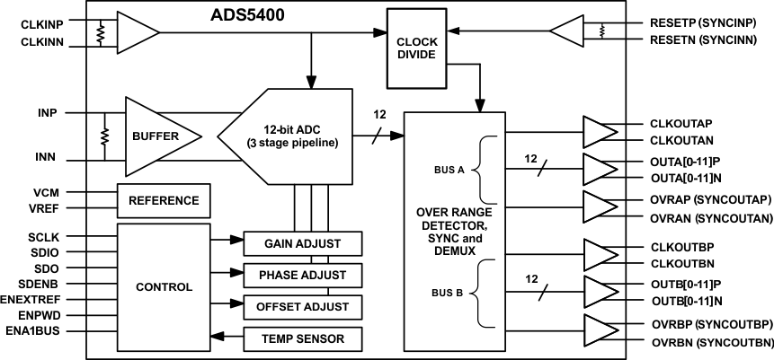
The ADS5400 is a 12-bit, 1-GSPS, monolithic pipeline ADC. Its bipolar transistor analog core operates from 5-V and 3.3-V supplies, while the output uses a 3.3-V supply to provide LVDS-compatible digital outputs. The conversion process is initiated by the falling edge of the external input clock. At the sampling instant, the differential input signal is captured by the input track-and-hold (T&H), and the input sample is sequentially converted by a series of lower resolution stages, with the outputs combined in a digital correction logic block. Both the rising and the falling clock edges are used to propagate the sample through the pipeline every half clock cycle. This process results in a data latency of 7 - 8.5 clock cycles (output mode dependent), after which the output data is available as a 12-bit parallel word, coded in offset binary or two's complement format.
The user can select to accept the data at the full sample rate using one bus (bus A, latency 7 cycles), or demultiplex the data into two buses (bus A and B, latency 7.5 or 8.5 cycles) at half rate. A serial peripheral interface (SPI) is provided for adjusting operational modes, as well as for calibrations of analog gain, analog offset and clock phase for inter-leaving multiple ADS5400. Die temperature readout using the SPI is provided. SYNC and RESET modes exist for synchronizing output data across multiple ADS5400.
7.2 Functional Block Diagram
7.3 Feature Description
7.3.1 Input Configuration
The analog input for the ADS5400 consists of an analog pseudo-differential buffer followed by a bipolar transistor track-and-hold (see Figure 25). The integrated analog buffer isolates the source driving the input of the ADC from sampling glitches on the T&H and allows for the integration of a 100-Ω differential input resistor. The input common mode is set internally through a 500-Ω resistor connected from half of the AVDD5 supply voltage to each of the inputs. The parasitic package capacitance shown is with the package unsoldered. Once soldered, depending on the board characteristics, one can expect another ~1pF at the analog input pins, which is board dependent.
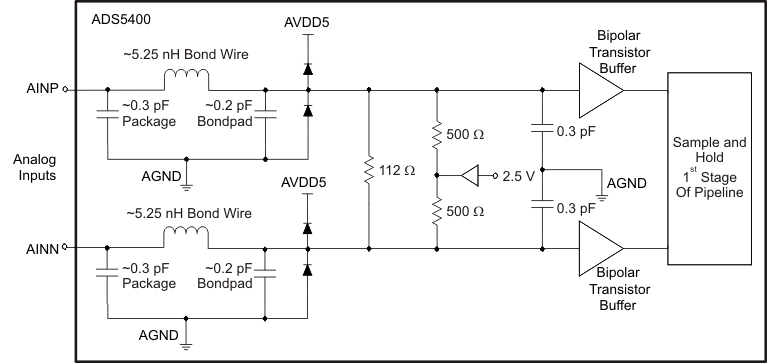 Figure 25. Analog Input Equivalent Circuit
For a full-scale differential input, each of the differential lines of the input signal swing symmetrically between 2.5 V + 0.5 V and 2.5 V – 0.5 V. This means that each input has a maximum signal swing of 1 VPP for a total differential input signal swing of 2 VPP. The maximum fullscale range can be programmed from 1.5 to 2 VPP using the SPI. The maximum swing is determined by the internal reference voltage generator and the fullscale range set using the SPI, eliminating the need for any external circuitry for this purpose. The analog gain adjustment has a resolution of 12-bits across the 1.5-2VPP range, providing for fine calibration of analog gain mismatches across multiple ADS5400 signal chains, primarily for interleaving.
The ADS5400 obtains optimum performance when the analog inputs are driven differentially. The circuit in Figure 26 shows one possible configuration using an RF transformer. Datasheet performance, especially at > 1-GHz input frequency, can only be obtained with a carefully designed differential drive path to the ADC.
 Figure 26. Converting a Single-Ended Input to a Differential Signal Using an RF Transformer
7.3.2 Voltage Reference
The 2 V voltage reference is provided internal to the ADS5400. A VCM (voltage common mode) pin is provided as an output for use in DC-coupled applications, equal to the AVDD5 supply divided by 2. This provides the analog input common mode voltage to a driving circuit so that the common mode is setup properly. Some systems may prefer the use of an external voltage reference. This mode can be enabled by pulling the ENEXTREF pin high. In this mode, an external reference can be driven onto the VREF pin, which is normally expecting 2 V.
7.3.3 Analog Input Over-Range Recovery Error
An over-range condition occurs if the analog input voltage exceeds the full-scale range of the converter (0 dBFS). To test recovery from an over-range, the ADC analog input is injected with a sinusoidal input frequency exactly at CLKIN/4 (a four-point sinusoid at the digital outputs). The four sample points of each period occur at the top, mid-scale, bottom and mid-scale of the sinusoid (clipped by the ADC when over-ranged to all 0s or all 1s). Once the amplitude exceeds 0dBFS, the top and bottom of the sinusoidal input becomes out of range, while the mid-scale point is always in-range and measureable with ADC output codes. The graph in Figure 27 indicates the amount of error from the expected mid-scale value of 2048 that occurs after negative over-range (bottom of sinusoid) and positive over-range (top of sinusoid). This equates to the amount of error in a valid sample 1 clock cycle after an over-range occurs, as a function of input amplitude.
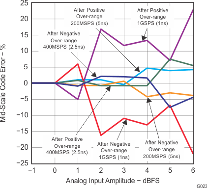 Figure 27. Recovery Error 1 Clock Cycle After Over-Range vs Input Amplitude
7.3.4 Clock Inputs
The ADS5400 clock input can be driven with either a differential clock signal or a single-ended clock input. The equivalent clock input circuit can be seen in Figure 28. In low-input-frequency applications, where jitter may not be a big concern, the use of a single-ended clock (as shown in Figure 29) could save cost and board space without much performance tradeoff. When clocked with this configuration, it is best to connect CLK to ground with a 0.01-μF capacitor, while CLK is ac-coupled with a 0.01-μF capacitor to the clock source, as shown in Figure 29.
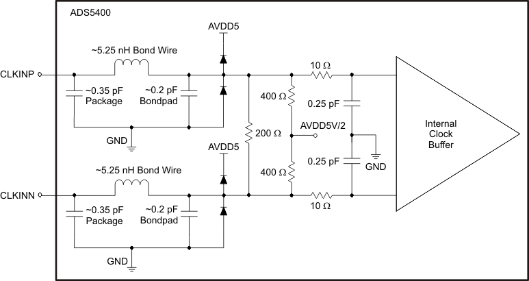 Figure 28. Clock Input Circuit
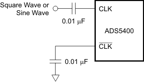 Figure 29. Single-Ended Clock
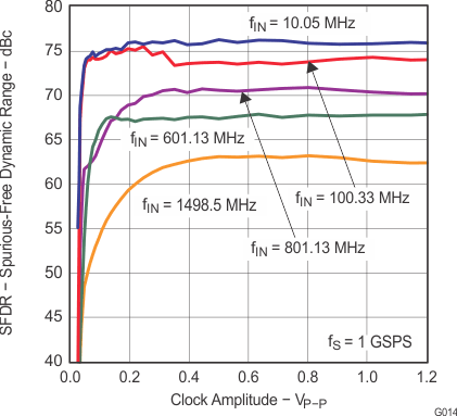 Figure 30. ADS5400 SFDR vs Differential Clock Level
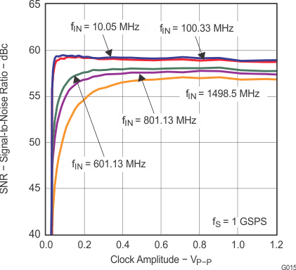 Figure 31. ADS5400 SNR vs Differential Clock Level
The characterization of the ADS5400 is typically performed with a 1.5 VPP differential clock, but the ADC performs well with a differential clock amplitude down to ~400 mVPP (200 mV swing on both CLK and CLK), as shown in Figure 30 and Figure 31. For jitter-sensitive applications, the use of a differential clock has some advantages at the system level and is strongly recommended. The differential clock allows for common-mode noise rejection at the printed circuit board (PCB) level. With a differential clock, the signal-to-noise ratio of the ADC is better for jitter-sensitive, high-frequency applications because the board level clock jitter is superior.
Larger clock amplitude levels are recommended for high analog input frequencies or slow clock frequencies. At high analog input frequencies, the sampling process is sensitive to jitter. At slow clock frequencies, a small amplitude sinusoidal clock has a lower slew rate and can create jitter-related SNR degradation due to the uncertainty in the sampling point associated with a slow slew rate. Figure 32 demonstrates a recommended method for converting a single-ended clock source into a differential clock; it is similar to the configuration found on the evaluation board and was used for much of the characterization. See also Clocking High Speed Data Converters (SLYT075) for more details.
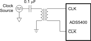 Figure 32. Differential Clock
The common-mode voltage of the clock inputs is set internally to 2.5 V using internal 400Ω resistors (see Figure 28). It is recommended to use ac coupling in the clock path, but if this scheme is not possible, the ADS5400 features good tolerance to clock common-mode variation, as shown in Figure 33 and Figure 34. The internal ADC core uses both edges of the clock for the conversion process. Ideally, a 50% duty-cycle clock signal should be provided.
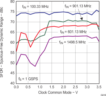 Figure 33. ADS5400 SFDR vs Clock Common Mode
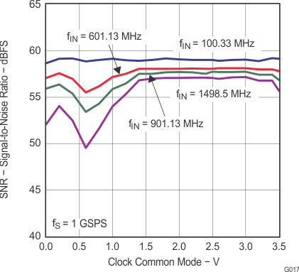 Figure 34. ADS5400 SNR vs Clock Common Mode
7.3.5 Over Range
The OVR output equals a logic high when the 12-bit output word attempts to exceed either all 0s or all 1s. This flag is provided as an indicator that the analog input signal exceeded the full-scale input limit set in register 0x00 and 0x01 (± gain error). The OVR indicator is provided for systems that use gain control to keep the analog input signal within acceptable limits. The OVR pins are not available when the sychronization mode is enabled, as they become the SYNCOUT indicator.
7.3.6 Data Scramble
In normal operation, with this mode disabled, the MSBs have similar energy to the analog input fundamental frequency and can in some instances cause board interference. A data scramble mode is available in register 0x06. In this mode, bits 11-1 are XOR'd with bit 0 (the LSB). Because of the random nature of the LSB, this has the effect of randomizing the data pattern. To de-scramble, perform the opposite operation in the digital chip after receiving the scrambled data.
7.3.7 Test Patterns
Determining the closure of timing or validating the digital interface can be difficult in normal operation. Therefore, test patterns are available in register 0x06. One pattern toggles the outputs between all 1s and all 0s. Another pattern generates a 7-bit PRBS (pseudo-random bit sequence).
In dual bus mode, the toggle mode could be in the same phase on bus A and B (bus A and B outputting 1s or 0s together), or could be out of phase (bus A outputting 1s while bus B outputs 0s). The start phase cannot be controlled.
The PRBS output sequence is a standard 27-1 pseudo-random sequence generated by a feedback shift register where the two last bits of the shift register are exclusive-OR’ed and fed back to the first bit of the shift register. The standard notation for the polynomial is x7 + x6 + 1. The PRBS generator is not reset, so there is no initial position in the sequence. The pattern may start at any position in the repeating 127-bit long pattern and the pattern repeats as long as the PRBS mode is enabled. The data pattern from the PRBS generator is used for all of the LVDS parallel outputs, so when the pattern is ‘1’ then all of the LVDS outputs are outputting ‘1’ and when the pattern is 0 then all of the LVDS drivers output 0. To determine if the digital interface is operating properly with the PRBS sequence, the user must generate the same sequence in the receiving device, and do a shift-and-compare until a matching sequence is confirmed.
7.3.8 Die Identification and Revision
A unique 64-bit die indentifier code can be read from registers 0x17 through 0x1E. An 8-bit die revision code is available in register 0x1F.
7.3.9 Die Temperature Sensor
In register 0x05, the die temperature sensor can be enabled. The sensor is power controlled independently of global powerdown, so that it and the SPI can be used to monitor the die temperature even when the remainder of the ADC is in sleep mode. Register 0x08 is used to read values which can be mapped to the die temperature. The exact mapping is detailed in the register map. Care should be taken not to exceed a maximum die temperature of 150°C for prolonged periods of time to maintain the life of the device.
7.3.10 Interleaving
7.3.10.1 Gain Adjustment
A signal gain adjustment is available in registers 0x00 and 0x01. The allowable fullscale range for the ADC is 1.52 - 2VPP and can be set with 12-bit adjustment resolution across this range. For equal up/down gain adjustment of the system and ADC gain mismatches, a nominal starting point of 1.75VPP could be programmed, in which case ±250 mV of adjustment range would be provided.
7.3.10.2 Offset Adjustment
Analog offset adjustment is available in register 0x03 and 0x04. This provides ±30 mV of adjustment range with 9-bit adjustment resolution of 120uV per step. At production test, the default code for this register setting is set to a value that provides 0 mV of ADC offset. For optimum spectral performance, it is not recommended to use more than ±8mV adjustment from the default setting
7.3.10.3 Input Clock Coarse Phase Adjustment
Coarse adjustment is available in register 0x02. The typical range is approximately 73 ps with a resolution of 2.4ps.
7.3.10.4 Input Clock Fine Phase Adjustment
Fine adjustment is available in register 0x03. The typical range is approximately 7.4 ps with a resolution of 116fs.
7.4 Device Functional Modes
7.4.1 Output Bus and Clock Options
The ADS5400 has two buses, A and B. Using register 0x02, a single or dual bus output can be selected. In single-bus mode, bus A is used at the full clock rate, while in two-bus mode, data is multiplexed at half the clock rate on A and B. While in single bus mode, CLKOUTA will be at frequency CLKIN/2 and a DDR interface is achieved. In two-bus mode, CLKOUTA/CLKOUTB can be either at frequency CLKIN/2 or CLKIN/4, providing options for an SDR or DDR interface. The ADC provides 12 LVDS-compatible data outputs (D11 to D0; D11 is the MSB and D0 is the LSB), a data-ready signal (CLKOUT), and an over-range indicator (OVR) on each bus. It is recommended to use the CLKOUT signal to capture the output data of the ADS5400. Both two's complement and offset binary are available output formats, in register 0x05.
The capacitive loading on the digital outputs should be minimized. Higher capacitance shortens the data-valid timing window. The values given for timing were obtained with an estimated 3.5-pF of differential parasitic board capacitance on each LVDS pair.
7.4.2 Reset and Synchronization
Referencing the timing diagrams starting in Figure 1, the polarity of CLKOUT with respect to the sample N data output transition is undetermined because of the unknown startup logic level of the clock divider that generates the CLKOUT signal, whether in frequency CLKIN/2 or CLKIN/4 mode. The polarity of CLKOUT could invert when power is cycled off/on. If a defined CLKOUT polarity is required, the RESET input pins are used to reset the clock divider to a known state after power on with a reset pulse. A RESET is not commonly required when using only one ADS5400 because a one sample uncertainty at startup is not usually a problem.
NOTE: initial samples capture RESET = HIGH on the rising edge of CLKINP. This is being corrected for final samples and will reflect the diagram as drawn, with RESET = HIGH captured on falling edge of CLKINP.
In addition to CLKOUT alignment using RESET, a synchronization mode is provided in register 0x05. In this mode, the OVR output becomes the SYNCOUT. The SYNCOUT will indicate which sample was present when the RESET input pulse was captured in a HIGH state. The OVR indicator is not available when sync mode is enabled. In single bus mode, only SYNCOUTA is used. In dual bus mode, only SYNCOUTB is used.
7.4.3 LVDS
Differential source loads of 100Ω and 200Ω are provided internal to the ADS5400 and can be implemented using register 0x06 (as well as no internal load). Normal LVDS operation expects 3.5 mA of current, but alternate values of 2.5, 4.5, and 5.5 mA are provided to save power or improve the LVDS signal quality when the environment provides excessive loading.
7.5 Programming
7.5.1 Serial Interface
The serial port of the ADS5400 is a flexible serial interface which communicates with industry standard microprocessors and microcontrollers. The interface provides read/write access to all registers used to define the operating modes of ADS5400. It is compatible with most synchronous transfer formats and can be configured as a 3 or 4 pin interface in register 0x01h. In both configurations, SCLK is the serial interface input clock and SDENB is serial interface enable. For 3 pin configuration, SDIO is a bidirectional pin for both data in and data out. For 4 pin configuration, SDIO is data in only and SDO is data out only.
Each read/write operation is framed by signal SDENB (Serial Data Enable Bar) asserted low for 2 to 5 bytes, depending on the data length to be transferred (1–4 bytes). The first frame byte is the instruction cycle which identifies the following data transfer cycle as read or write, how many bytes to transfer, and what address to transfer the data. Table 1 indicates the function of each bit in the instruction cycle and is followed by a detailed description of each bit. Frame bytes 2 to 5 comprise the data transfer cycle.
Table 1. Instruction Byte of the Serial Interface
| MSB | LSB | |||||||
|---|---|---|---|---|---|---|---|---|
| Bit | 7 | 6 | 5 | 4 | 3 | 2 | 1 | 0 |
| Description | R/W | N1 | N0 | A4 | A3 | A2 | A1 | A0 |
| R/W | Identifies the following data transfer cycle as a read or write operation. A high indicates a read operation from ADS5400 and a low indicates a write operation to the ADS5400. | |||||||
| [N1:N0] | Identifies the number of data bytes to be transferred per Table 2. Data is transferred MSB first. | |||||||
| [A4:A0] | Identifies the address of the register to be accessed during the read or write operation. For multi-byte transfers, this address is the starting address. Note that the address is written to the ADS5400 MSB first and counts down for each byte. | |||||||
Table 2. Number of Transferred Bytes Within One Communication Frame
| N1 | N0 | Description |
|---|---|---|
| 0 | 0 | Transfer 1 Byte |
| 0 | 1 | Transfer 2 Bytes |
| 1 | 0 | Transfer 3 Bytes |
| 1 | 1 | Transfer 4 Bytes |
Figure 35 shows the serial interface timing diagram for a ADS5400 write operation. SCLK is the serial interface clock input to ADS5400. Serial data enable SDENB is an active low input to ADS5400. SDIO is serial data in. Input data to ADS5400 is clocked on the rising edges of SCLK.
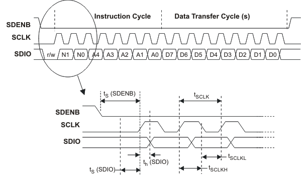 Figure 35. Serial Interface Write Timing Diagram
Figure 36 shows the serial interface timing diagram for a ADS5400 read operation. SCLK is the serial interface clock input to ADS5400. Serial data enable SDENB is an active low input to ADS5400. SDIO is serial data in during the instruction cycle. In 3 pin configuration, SDIO is data out from ADS5400 during the data transfer cycle(s), while SDO is in a high-impedance state. In 4 pin configuration, SDO is data out from ADS5400 during the data transfer cycle(s). At the end of the data transfer, SDO will output low on the final falling edge of SCLK until the rising edge of SDENB when it will 3-state.
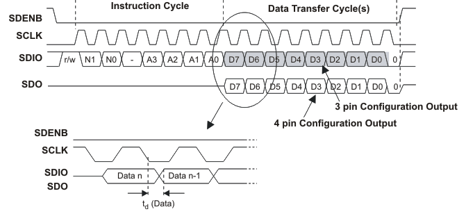 Figure 36. Serial Interface Read Timing Diagram
7.6 Register Maps
7.6.1 Serial Register Map
Table 3 gives a summary of all the modes that can be programmed through the serial interface.
Table 3. Summary of Functions Supported by Serial Interface
| REGISTER ADDRESS IN HEX |
REGISTER FUNCTIONS | ||||||||
|---|---|---|---|---|---|---|---|---|---|
| Address | BIT 7 | BIT 6 | BIT 5 | BIT 4 | BIT 3 | BIT 2 | BIT 1 | BIT 0 | |
| 00 | Analog Gain Adjustment bits<11:4> | ||||||||
| 01 | continued...Analog Gain Adjustment bits<3:0> | 3 or 4-pin SPI | SPI Reset | 0 | 0 | ||||
| 02 | Coarse Clock Phase Adjustment bits<4:0> | 0 | Clock Divider | Single or Dual Bus | |||||
| 03 | Fine Clock Phase Adjustment bits<5:0> | 0 | Analog Offset bit<8> | ||||||
| 04 | continued...Analog Offset Control bits<7:0> | ||||||||
| 05 | Temp Sensor | Powerdown | 1 | Sync Mode | Data Format | Reference | Stagger Output | 0 | |
| 06 | Data output mode | LVDS termination | LVDS current | Force LVDS outputs | |||||
| 07 | 0000 0000 | ||||||||
| 08 | Die temperature bits<7:0> | ||||||||
| 09 | 000 0000 | Memory error | |||||||
| 0A | 0000 0000 | ||||||||
| 0B-16 | addresses not implemented, writes have no effect, reads return 0x00 | ||||||||
| 17 | DIE ID<7:0> | ||||||||
| 18 | DIE ID<15:8> | ||||||||
| 19 | DIE ID<23:16> | ||||||||
| 1A | DIE ID<31:24> | ||||||||
| 1B | DIE ID<39:32> | ||||||||
| 1C | DIE ID<47:40> | ||||||||
| 1D | DIE ID<55:48> | ||||||||
| 1E | DIE ID<63:56> | ||||||||
| 1F | Die revision indicator<7:0> | ||||||||
7.6.2 Description of Serial Registers
This section explains each register function in detail.
Table 4. Serial Register 0x00 (Read or Write)
| Address (hex) | BIT 7 | BIT 6 | BIT 5 | BIT 4 | BIT 3 | BIT 2 | BIT 1 | BIT 0 |
|---|---|---|---|---|---|---|---|---|
| 0x00 | Analog Gain Adjustment bits<11:4> | |||||||
| Defaults | 0 | 0 | 0 | 0 | 0 | 0 | 0 | 0 |
| BIT <7:0> | Analog gain adjustment (most significant 8 bits of a 12 bit word) | |
| All 12-bits in this adjustment in address 0x00 and 0x01 set to 0000 0000 0000 = full-scale analog input 2.0VPP | ||
| All 12-bits in this adjustment in address 0x00 and 0x01 set to 1111 1111 1111 = full-scale analog input 1.52VPP | ||
| Step adjustment resolution is 120µV. | ||
| Can be used for one-time setting or continual calibration of analog signal path gain. | ||
Table 5. Serial Register 0x01 (Read or Write)
| Address (hex) | BIT 7 | BIT 6 | BIT 5 | BIT 4 | BIT 3 | BIT 2 | BIT 1 | BIT 0 |
|---|---|---|---|---|---|---|---|---|
| 0x01 | Analog Gain Adjustment bits<3:0> | 3 or 4-pin SPI | SPI Reset | 0 | 0 | |||
| Defaults | 0 | 0 | 0 | 0 | 0 | 0 | 0 | 0 |
Table 6. Serial Register 0x02 (Read or Write)
| Address (hex) | BIT 7 | BIT 6 | BIT 5 | BIT 4 | BIT 3 | BIT 2 | BIT 1 | BIT 0 |
|---|---|---|---|---|---|---|---|---|
| 0x02 | Coarse Clock Phase Adjustment bits<4:0> | 0 | Clock Divider | Single or Dual Bus | ||||
| Defaults | 0 | 0 | 0 | 0 | 0 | 0 | 0 | 0 |
Table 7. Serial Register 0x03 (Read or Write)
| Address (hex) | BIT 7 | BIT 6 | BIT 5 | BIT 4 | BIT 3 | BIT 2 | BIT 1 | BIT 0 |
|---|---|---|---|---|---|---|---|---|
| 0x03 | Fine Clock Phase Adjustment bits<5:0> | 0 | Analog Offset bit<8> | |||||
| Defaults | 0 | 0 | 0 | 0 | 0 | 0 | 0 | factory set |
Table 8. Serial Register 0x04 (Read or Write)
| Address (hex) | BIT 7 | BIT 6 | BIT 5 | BIT 4 | BIT 3 | BIT 2 | BIT 1 | BIT 0 |
|---|---|---|---|---|---|---|---|---|
| 0x04 | Analog Offset Control bits<7:0> | |||||||
| Defaults | factory set | |||||||
Table 9. Serial Register 0x05 (Read or Write)
| Address (hex) | BIT 7 | BIT 6 | BIT 5 | BIT 4 | BIT 3 | BIT 2 | BIT 1 | BIT 0 |
|---|---|---|---|---|---|---|---|---|
| 0x05 | Temp Sensor | Powerdown | reserved | Sync Mode | Data Format | Reference | Stagger Output | 0 |
| Defaults | 0 | 0 | 1 | 0 | 0 | 0 | 0 | 0 |
| BIT <0> | RESERVED | |
| 0 | set to 0 if writing this register | |
| 1 | do not set to 1 | |
| BIT <1> | Stagger Output Bus | |
| 0 | Output bus A and B aligned | |
| 1 | Output bus A and B staggered (see timing diagrams) | |
| BIT <2> | Enable External Reference | |
| 0 | Enable internal reference | |
| 1 | Enable external reference | |
| BIT <3> | Set Data Output Format | |
| 0 | Enable offset binary | |
| 1 | Enable two's complement | |
| BIT <4> | Set Sync Mode | |
| 0 | Disable data synchronization mode | |
| 1 | Enable data synchronization mode | |
| When enabled, the OVR pins are replaced with SYNC output signals. The SYNC output signal is time-aligned with the output data matching the corresponding input sample and RESET input pulse | ||
| BIT <5> | RESERVED | |
| 0 | ||
| 1 | set to 1 if writing this register | |
| BIT <6> | Powerdown | |
| 0 | device active | |
| 1 | device in low power mode (sleep mode) | |
| BIT <7> | Temperature Sensor | |
| 0 | temperature sensor inactive | |
| 1 | temperature sensor active, independent of powerdown bit in Bit<6>, allows reading of temp sensor while the rest of the ADC is in sleep mode | |
Table 10. Serial Register 0x06 (Read or Write)
| Address (hex) | BIT 7 | BIT 6 | BIT 5 | BIT 4 | BIT 3 | BIT 2 | BIT 1 | BIT 0 |
|---|---|---|---|---|---|---|---|---|
| 0x06 | Data output mode | LVDS termination | LVDS current | Force LVDS outputs | ||||
| Defaults | 0 | 0 | 0 | 0 | 0 | 1 | 0 | 0 |
Table 11. Serial Register 0x08 (Read only)
| Address (hex) | BIT 7 | BIT 6 | BIT 5 | BIT 4 | BIT 3 | BIT 2 | BIT 1 | BIT 0 |
|---|---|---|---|---|---|---|---|---|
| 0x08 | Die temperature bits<7:0> | |||||||
| Defaults | depends on reading from temperature sensor | |||||||
| BIT <7:0> | Die temperature readout | |
| if enabled in register 0x05. To obtain the die temperature in Celsius, convert the 8-bit word to decimal and subtract 78. | ||
| <7:0> = 0x00 = 00000000, measured temperature is 0 – 78 = –78°C | ||
| <7:0> = 0x73 = 01110011, measured temperature is 115 – 78 = 37°C | ||
| <7:0> = 0xAF, measured temperature is 175 – 78 = 97°C | ||
Table 12. Serial Register 0x09 (Read only)
| Address (hex) | BIT 7 | BIT 6 | BIT 5 | BIT 4 | BIT 3 | BIT 2 | BIT 1 | BIT 0 |
|---|---|---|---|---|---|---|---|---|
| 0x09 | 000 0000 | Memory error | ||||||
| Defaults | 000 0000 | 0 | ||||||
| BIT <7:1> | RESERVED | |
| set to 0 if writing this register | ||
| do not set to 1 | ||
| BIT <0> | Memory Error Indicator | |
| Registers 0x00 through 0x07 have multiple redundancy. If any copy disagrees with the others, an error is flagged in this bit. This is for systems that require the highest level of assurance that the device remains programmed in the proper state and indication of an error if something changes unexpectedly. | ||
Table 13. Serial Register 0x0A (Read only)
| Address (hex) | BIT 7 | BIT 6 | BIT 5 | BIT 4 | BIT 3 | BIT 2 | BIT 1 | BIT 0 |
|---|---|---|---|---|---|---|---|---|
| 0x0A | 0000 0000 | |||||||
| Defaults | 0000 0000 | |||||||
| BIT <7:0> | RESERVED | |
| set to 0 if writing this register | ||
| do not set to 1 | ||
Table 14. Serial Register 0x17 through 0x1E (Read only)
| Address (hex) | BIT 7 | BIT 6 | BIT 5 | BIT 4 | BIT 3 | BIT 2 | BIT 1 | BIT 0 |
|---|---|---|---|---|---|---|---|---|
| 0x17 - 0x1E | Die ID | |||||||
| Defaults | factory set | |||||||
| BIT <7:0> | Die Identification Bits | |
| Each of these eight registers contains 8-bits of a 64-bit unique die identifier. | ||
Table 15. Serial Register 0x1F (Read only)
| Address (hex) | BIT 7 | BIT 6 | BIT 5 | BIT 4 | BIT 3 | BIT 2 | BIT 1 | BIT 0 |
|---|---|---|---|---|---|---|---|---|
| 0x1F | Die Revision Number | |||||||
| Defaults | factory set | |||||||
| BIT <7:0> | Die revision | |
| Provides design revision information. | ||