ZHCSEA4C May 2015 – December 2020 ADS54J40
PRODUCTION DATA
- 1 特性
- 2 应用
- 3 说明
- 4 Revision History
- 5 ADS54J40 Comparison
- 6 Pin Configuration and Functions
- 7 Specifications
-
8 Detailed Description
- 8.1 Overview
- 8.2 Functional Block Diagram
- 8.3 Feature Description
- 8.4 Device Functional Modes
- 8.5
Register Maps
- 8.5.1 Example Register Writes
- 8.5.2
Register Descriptions
- 8.5.2.1 General Registers
- 8.5.2.2
Master Page (080h) Registers
- 8.5.2.2.1 Register 20h (address = 20h), Master Page (080h)
- 8.5.2.2.2 Register 21h (address = 21h), Master Page (080h)
- 8.5.2.2.3 Register 23h (address = 23h), Master Page (080h)
- 8.5.2.2.4 Register 24h (address = 24h), Master Page (080h)
- 8.5.2.2.5 Register 26h (address = 26h), Master Page (080h)
- 8.5.2.2.6 Register 4Fh (address = 4Fh), Master Page (080h)
- 8.5.2.2.7 Register 53h (address = 53h), Master Page (080h)
- 8.5.2.2.8 Register 54h (address = 54h), Master Page (080h)
- 8.5.2.2.9 Register 55h (address = 55h), Master Page (080h)
- 8.5.2.2.10 Register 59h (address = 59h), Master Page (080h)
- 8.5.2.3 ADC Page (0Fh) Register
- 8.5.2.4
Main Digital Page (6800h) Registers
- 8.5.2.4.1 Register 0h (address = 0h), Main Digital Page (6800h)
- 8.5.2.4.2 Register 40h (address = 40h), Main Digital Page (6800h)
- 8.5.2.4.3 Register 41h (address = 41h), Main Digital Page (6800h)
- 8.5.2.4.4 Register 42h (address = 42h), Main Digital Page (6800h)
- 8.5.2.4.5 Register 43h (address = 43h), Main Digital Page (6800h)
- 8.5.2.4.6 Register 44h (address = 44h), Main Digital Page (6800h)
- 8.5.2.4.7 Register 4Bh (address = 4Bh), Main Digital Page (6800h)
- 8.5.2.4.8 Register 4Dh (address = 4Dh), Main Digital Page (6800h)
- 8.5.2.4.9 Register 4Eh (address = 4Eh), Main Digital Page (6800h)
- 8.5.2.4.10 Register 52h (address = 52h), Main Digital Page (6800h)
- 8.5.2.4.11 Register 68h (address = 68h), Main Digital Page (6800h)
- 8.5.2.4.12 Register 72h (address = 72h), Main Digital Page (6800h)
- 8.5.2.4.13 Register ABh (address = ABh), Main Digital Page (6800h)
- 8.5.2.4.14 Register ADh (address = ADh), Main Digital Page (6800h)
- 8.5.2.4.15 Register F7h (address = F7h), Main Digital Page (6800h)
- 8.5.2.5
JESD Digital Page (6900h) Registers
- 8.5.2.5.1 Register 0h (address = 0h), JESD Digital Page (6900h)
- 8.5.2.5.2 Register 1h (address = 1h), JESD Digital Page (6900h)
- 8.5.2.5.3 Register 2h (address = 2h), JESD Digital Page (6900h)
- 8.5.2.5.4 Register 3h (address = 3h), JESD Digital Page (6900h)
- 8.5.2.5.5 Register 5h (address = 5h), JESD Digital Page (6900h)
- 8.5.2.5.6 Register 6h (address = 6h), JESD Digital Page (6900h)
- 8.5.2.5.7 Register 7h (address = 7h), JESD Digital Page (6900h)
- 8.5.2.5.8 Register 16h (address = 16h), JESD Digital Page (6900h)
- 8.5.2.5.9 Register 31h (address = 31h), JESD Digital Page (6900h)
- 8.5.2.5.10 Register 32h (address = 32h), JESD Digital Page (6900h)
- 8.5.2.6
JESD Analog Page (6A00h) Registers
- 8.5.2.6.1 Register 12h (address = 12h), JESD Analog Page (6A00h)
- 8.5.2.6.2 Registers 13h-15h (addresses = 13h-5h), JESD Analog Page (6A00h)
- 8.5.2.6.3 Register 16h (address = 16h), JESD Analog Page (6A00h)
- 8.5.2.6.4 Register 17h (address = 17h), JESD Analog Page (6A00h)
- 8.5.2.6.5 Register 1Ah (address = 1Ah), JESD Analog Page (6A00h)
- 8.5.2.6.6 Register 1Bh (address = 1Bh), JESD Analog Page (6A00h)
- 8.5.2.7
Offset Read Page (JESD BANK PAGE SEL = 6100h, JESD BANK PAGE SEL1
= 0000h) Registers
- 8.5.2.7.1 Register 068h (address = 068h), Offset Read Page
- 8.5.2.7.2 Register 069h (address = 069h), Offset Read Page
- 8.5.2.7.3 Registers 074h, 076h, 078h, 7Ah (address = 074h, 076h, 078h, 7Ah), Offset Read Page
- 8.5.2.7.4 Registers 075h, 077h, 079h, 7Bh (address = 075h, 077h, 079h, 7Bh), Offset Read Page
- 8.5.2.8 Offset Load Page (JESD BANK PAGE SEL= 6100h, JESD BANK PAGE SEL1 = 0500h) Registers
- 9 Application Information Disclaimer
- 10Power Supply Recommendations
- 11Layout
- 12Device and Documentation Support
8.3.1 Analog Inputs
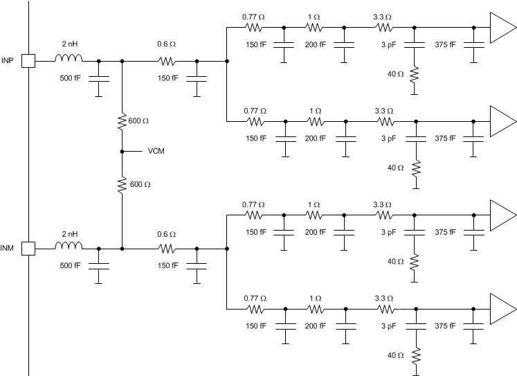
The ADS54J40 analog signal inputs are designed to be driven differentially. The analog input pins have internal analog buffers that drive the sampling circuit. As a result of the analog buffer, the input pins present a high impedance input across a very wide frequency range to the external driving source that enables great flexibility in the external analog filter design as well as excellent 50-Ω matching for RF applications. The buffer also helps isolate the external driving circuit from the internal switching currents of the sampling circuit, resulting in a more constant SFDR performance across input frequencies.
The common-mode voltage of the signal inputs is internally biased to VCM using 600-Ω resistors, allowing for ac-coupling of the input drive network. Each input pin (INP, INM) must swing symmetrically between (VCM +
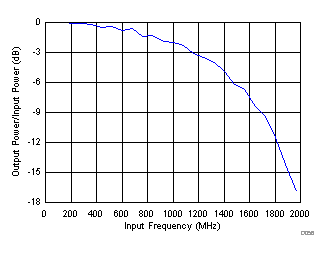
0.475 V) and (VCM – 0.475 V), resulting in a 1.9-VPP (default) differential input swing. The input sampling circuit has a 3-dB bandwidth that extends up to 1.2 GHz. An equivalent analog input network diagram is shown in Figure 8-1.
 Figure 8-1 Analog Input Network
The input bandwidth shown in Figure 8-2 is measured with respect to a 50-Ω differential input termination at the ADC input pins. Figure x shows the signal processing done inside the DDC block of the ADS54J40.
 Figure 8-2 Transfer Function vs Frequency