ZHCSH75A September   2017  – December 2017 ADS7142

PRODUCTION DATA.  

  1. 特性
  2. 应用
  3. 说明
    1.     Device Images
  4. 修订历史记录
  5. Pin Configuration and Functions
    1.     Pin Functions
  6. Specifications
    1. 6.1  Absolute Maximum Ratings
    2. 6.2  ESD Ratings
    3. 6.3  Recommended Operating Conditions
    4. 6.4  Thermal Information
    5. 6.5  Electrical Characteristics - All Modes
    6. 6.6  Electrical Characteristics - Manual Mode
    7. 6.7  Electrical Characteristics - Autonomous Modes
    8. 6.8  Electrical Characteristics - High Precision Mode
    9. 6.9  Timing Requirements
    10. 6.10 Switching Characteristics
    11. 6.11 Typical Characteristics for All Modes
    12. 6.12 Typical Characteristics for Manual Mode
    13. 6.13 Typical Characteristics for Autonomous Modes
    14. 6.14 Typical Characteristics for High Precision Mode
  7. Detailed Description
    1. 7.1 Overview
    2. 7.2 Functional Block Diagram
    3. 7.3 Feature Description
      1. 7.3.1  Analog Input and Multiplexer
        1. 7.3.1.1 Two-Channel, Single-Ended Configuration
        2. 7.3.1.2 Single-Channel, Single-Ended Configuration
        3. 7.3.1.3 Single-Channel, Pseudo-Differential Configuration
      2. 7.3.2  OFFSET Calibration
      3. 7.3.3  Reference
      4. 7.3.4  ADC Transfer Function
      5. 7.3.5  Oscillator and Timing Control
      6. 7.3.6  I2C Address Selector
      7. 7.3.7  Data Buffer
        1. 7.3.7.1 Filling of the Data Buffer
        2. 7.3.7.2 Reading data from the Data Buffer
      8. 7.3.8  Accumulator
      9. 7.3.9  Digital Window Comparator
      10. 7.3.10 I2C Protocol Features
        1. 7.3.10.1 General Call
        2. 7.3.10.2 General Call with Software Reset
        3. 7.3.10.3 General Call with Write Software programmable part of slave address
        4. 7.3.10.4 Configuring Device into High Speed I2C mode
        5. 7.3.10.5 Bus Clear
      11. 7.3.11 Device Programming
        1. 7.3.11.1 Reading Registers
          1. 7.3.11.1.1 Single Register Read
          2. 7.3.11.1.2 Reading a Continuous Block of Registers
        2. 7.3.11.2 Writing Registers
          1. 7.3.11.2.1 Single Register Write
          2. 7.3.11.2.2 Set Bit
          3. 7.3.11.2.3 Clear Bit
          4. 7.3.11.2.4 Writing a continuous block of registers
    4. 7.4 Device Functional Modes
      1. 7.4.1 Device Power Up and Reset
      2. 7.4.2 Manual Mode
        1. 7.4.2.1 Manual Mode with CH0 Only
        2. 7.4.2.2 Manual Mode with AUTO Sequence
      3. 7.4.3 Autonomous Modes
        1. 7.4.3.1 Autonomous Mode with Threshold Monitoring and Diagnostics
          1. 7.4.3.1.1 Autonomous Mode with Pre Alert Data
          2. 7.4.3.1.2 Autonomous Mode with Post Alert Data
        2. 7.4.3.2 Autonomous Mode with Burst Data
          1. 7.4.3.2.1 Autonomous Mode with Start Burst
          2. 7.4.3.2.2 Autonomous Mode with Stop Burst
      4. 7.4.4 High Precision Mode
    5. 7.5 Optimizing Power Consumed by the Device
    6. 7.6 Register Map
      1. 7.6.1 RESET REGISTERS
        1. 7.6.1.1 WKEY Register (address = 17h), [reset = 00h]
          1. Table 6. WKEY Register Field Descriptions
        2. 7.6.1.2 DEVICE_RESET Register (address = 14h), [reset = 00h]
          1. Table 7. DEVICE_RESET Register Field Descriptions
      2. 7.6.2 FUNCTIONAL MODE SELECT REGISTERS
        1. 7.6.2.1 OFFSET_CAL Register (address = 15h), [reset = 00h]
          1. Table 8. OFFSET_CAL Register Field Descriptions
        2. 7.6.2.2 OPMODE_SEL Register (address = 1Ch), [reset = 00h]
          1. Table 9. OPMODE_SEL Register Field Descriptions
        3. 7.6.2.3 OPMODE_I2CMODE_STATUS Register (address = 00h), [reset = 00h]
          1. Table 10. OPMODE_I2CMODE_STATUS Register Field Descriptions
      3. 7.6.3 INPUT CONFIG REGISTER
        1. 7.6.3.1 CHANNEL_INPUT_CFG Register (address = 24h), [reset = 00h]
          1. Table 11. CHANNEL_INPUT_CFG Register Field Descriptions
      4. 7.6.4 ANALOG MUX and SEQUENCER REGISTERS
        1. 7.6.4.1 AUTO_SEQ_CHEN Register (address = 20h), [reset = 03h]
          1. Table 12. AUTO_SEQ_CHEN Register Field Descriptions
        2. 7.6.4.2 START_SEQUENCE Register (address = 1Eh), [reset = 00h]
          1. Table 13. START_SEQUENCE Register Field Descriptions
        3. 7.6.4.3 ABORT_SEQUENCE Register (address = 1Fh), [reset = 00h]
          1. Table 14. ABORT_SEQUENCE Register Field Descriptions
        4. 7.6.4.4 SEQUENCE_STATUS Register (address = 04h), [reset = 00h]
          1. Table 15. SEQUENCE_STATUS Register Field Descriptions
      5. 7.6.5 OSCILLATOR and TIMING CONTROL REGISTERS
        1. 7.6.5.1 OSC_SEL Register (address = 18h), [reset = 00h]
          1. Table 16. OSC_SEL Register Field Descriptions
        2. 7.6.5.2 nCLK_SEL Register (address = 19h), [reset = 00h]
          1. Table 17. nCLK_SEL Register Field Descriptions
      6. 7.6.6 DATA BUFFER CONTROL REGISTER
        1. 7.6.6.1 DATA_BUFFER_OPMODE Register (address = 2Ch), [reset = 01h]
          1. Table 18. DATA_BUFFER_OPMODE Register Field Descriptions
        2. 7.6.6.2 DOUT_FORMAT_CFG Register (address = 28h), [reset = 00h]
          1. Table 19. DOUT_FORMAT_CFG Register Field Descriptions
        3. 7.6.6.3 DATA_BUFFER_STATUS Register (address = 01h), [reset = 00h]
          1. Table 20. DATA_BUFFER_STATUS Register Field Descriptions
      7. 7.6.7 ACCUMULATOR CONTROL REGISTERS
        1. 7.6.7.1 ACC_EN Register (address = 30h), [reset = 00h]
          1. Table 21. ACC_EN Register Field Descriptions
        2. 7.6.7.2 ACC_CH0_LSB Register (address = 08h), [reset = 00h]
          1. Table 22. ACC_CH0_LSB Register Field Descriptions
        3. 7.6.7.3 ACC_CH0_MSB Register (address = 09h), [reset = 00h]
          1. Table 23. ACC_CH0_MSB Register Field Descriptions
        4. 7.6.7.4 ACC_CH1_LSB Register (address = 0Ah), [reset = 00h]
          1. Table 24. ACC_CH1 LSB Register Field Descriptions
        5. 7.6.7.5 ACC_CH1_MSB Register (address = 0Bh), [reset = 00h]
          1. Table 25. ACC_CH1 MSB Register Field Descriptions
        6. 7.6.7.6 ACCUMULATOR_STATUS Register (address = 02h), [reset = 00h]
          1. Table 26. ACCUMULATOR_STATUS Register Field Descriptions
      8. 7.6.8 DIGITAL WINDOW COMPARATOR REGISTERS
        1. 7.6.8.1  ALERT_DWC_EN Register (address = 37h), [reset = 00h]
          1. Table 27. ALERT_DWC_EN Register Field Descriptions
        2. 7.6.8.2  ALERT_CHEN (address = 34h), [reset = 00h]
          1. Table 28. ALERT_CHEN Register Field Descriptions
        3. 7.6.8.3  DWC_HTH_CH0_MSB Register (address = 39h), [reset = 00h]
          1. Table 29. DWC_HTH_CH0_LSB Register Field Descriptions
        4. 7.6.8.4  DWC_HTH_CH0_LSB Register (address = 38h), [reset = 00h]
          1. Table 30. DWC_HTH_CH0_LSB Register Field Descriptions
        5. 7.6.8.5  DWC_LTH_CH0_MSB Register (address = 3Bh), [reset = 00h]
          1. Table 31. DWC_LTH_CH0_MSB Register Field Descriptions
        6. 7.6.8.6  DWC_LTH_CH0_LSB Register (address = 3Ah), [reset = 00h]
          1. Table 32. DWC_LTH_CH0_LSB Register Field Descriptions
        7. 7.6.8.7  DWC_HYS_CH0 (address = 40h), [reset = 00h]
          1. Table 33. DWC_HYS_CH0 Register Field Descriptions
        8. 7.6.8.8  DWC_HTH_CH1_MSB Register (address = 3Dh), [reset = 00h]
          1. Table 34. DWC_HTH_CH1_LSB Register Field Descriptions
        9. 7.6.8.9  DWC_HTH_CH1_LSB Register (address = 3Ch), [reset = 00h]
          1. Table 35. DWC_HTH_CH1_LSB Register Field Descriptions
        10. 7.6.8.10 DWC_LTH_CH1_MSB Register (address = 3Fh), [reset = 00h]
          1. Table 36. DWC_LTH_CH1_MSB Register Field Descriptions
        11. 7.6.8.11 DWC_LTH_CH1_LSB Register (address = 3Eh), [reset = 00h]
          1. Table 37. DWC_LTH_CH1_LSB Register Field Descriptions
        12. 7.6.8.12 DWC_HYS_CH1 (address = 41h), [reset = 00h]
          1. Table 38. DWC_HYS_CH1 Register Field Descriptions
        13. 7.6.8.13 PRE_ALT_MAX_EVENT_COUNT Register (address = 36h), [reset = 00h]
          1. Table 39. PRE_ALT_MAX_EVENT_COUNT Register Field Descriptions
        14. 7.6.8.14 ALERT_TRIG_CHID Register (address = 03h), [reset = 00h]
          1. Table 40. ALERT_TRIG_CHID Register Field Descriptions
        15. 7.6.8.15 ALERT_LOW_FLAGS Register (address = 0C), [reset = 00h]
          1. Table 41. ALERT_LOW_FLAGS Register Field Descriptions
        16. 7.6.8.16 ALERT_HIGH_FLAGS Register (address = 0Eh), [reset = 00h]
          1. Table 42. ALERT_HIGH_FLAGS Register Field Descriptions
  8. Application and Implementation
    1. 8.1 Application Information
    2. 8.2 Typical Applications
      1. 8.2.1 ADS7142 as a Programmable Comparator with False Trigger Prevention and Diagnostics
        1. 8.2.1.1 Design Requirements
          1. 8.2.1.1.1 Higher Power Consumption
          2. 8.2.1.1.2 Fixed Threshold Voltages
        2. 8.2.1.2 Detailed Design Procedure
          1. 8.2.1.2.1 Programmable Thresholds and Hysteresis
          2. 8.2.1.2.2 False Trigger Prevention with Event Counter
          3. 8.2.1.2.3 Fault Diagnostics with Data Buffer
        3. 8.2.1.3 Application Curve
      2. 8.2.2 Event-triggered PIR sensing with ADS7142
        1. 8.2.2.1 Design Requirements
        2. 8.2.2.2 Detailed Design Procedure
        3. 8.2.2.3 Application Curves
  9. Power-Supply Recommendations
    1. 9.1 AVDD and DVDD Supply Recommendations
  10. 10Layout
    1. 10.1 Layout Guidelines
    2. 10.2 Layout Example
  11. 11器件和文档支持
    1. 11.1 文档支持
    2. 11.2 接收文档更新通知
    3. 11.3 社区资源
    4. 11.4 商标
    5. 11.5 静电放电警告
    6. 11.6 Glossary
  12. 12机械、封装和可订购信息

封装选项

机械数据 (封装 | 引脚)
散热焊盘机械数据 (封装 | 引脚)
订购信息

High Precision Mode

The High Precision Mode increases the accuracy of the data measurement to 16-bit accuracy. This is useful for applications where the level of precision required to accurately measure the sensor output needs to be higher than 12 bits. Applications that could take advantage of this type of functionality include gas detectors, air quality testers, water quality testers, and so on.

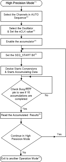
For this mode, Set OPMODE_SEL register to 111b. In this mode, the device starts converting and starts accumulating the conversion results in an accumulator on setting the SEQ_START bit. The device stops accumulating the conversion results in accumulator after 16 conversions or when the SEQ_ABORT bit is set. Upon accumulating 16 twelve bit conversions, the accumulator contains one 16 bit conversion result. The device has an accumulator for each channel and the device accumulates conversion results from each channel into the respective accumulator. If the operation of the device is aborted in high precision mode before the BUSY/RDY pin goes low, the device provides invalid data. In this mode, on providing a device address and read bit for reading data buffer (Figure 46), the device provides zeroes as output. In this mode, the BUSY/RDY can be used to wake up the MCU or host from sleep or hibernation on completion of accumulation. The steps for configuring the device into High Precision Mode are illustrated in Figure 66 .
ADS7142 fc_high_prec_mode_sbas773.gif
For setting the operation mode to High Precision mode, Refer to Figure 54
Select the channels in the AUTO_SEQ_CFG register.
Select the oscillator by configuring the OSC_SEL register and configure the nCLK register.
Enable the accumulator by setting bits in the ACC_EN register.
Set the bit SEQ_START bit in the START_SEQUENCE register.
Read the ACC_CHx_xxx registers.
Select another operation mode in the OPMODE_SEL register.
For reading and writing registers, Refer to Device Programming section.
Figure 66. Configuring Device in High Precision Mode

It is recommended to abort the present sequence by setting the SEQ_ABORT bit before changing the device operation mode or device configuration.

Figure 67 illustrates the accumulation of conversion results in high precision mode.
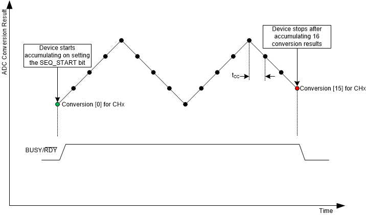
ADS7142 high_prec_mode_sbas773.gifFigure 67. High Precision Mode with Single Channel Configurations
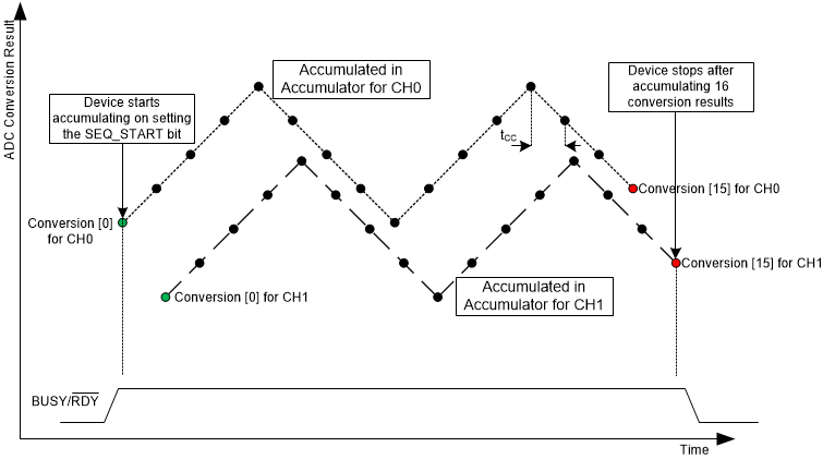
ADS7142 high_prec_mode_dual_channel_sbas773.gifFigure 68. High Precision Mode with Dual Channel Configurations