SBAS404D October 2006 – February 2016 ADS8556 , ADS8557 , ADS8558
PRODUCTION DATA.
- 1 Features
- 2 Applications
- 3 Description
- 4 Revision History
- 5 Pin Configuration and Functions
-
6 Specifications
- 6.1 Absolute Maximum Ratings
- 6.2 ESD Ratings
- 6.3 Recommended Operating Conditions
- 6.4 Thermal Information
- 6.5 Electrical Characteristics: General
- 6.6 Electrical Characteristics: ADS8556
- 6.7 Electrical Characteristics: ADS8557
- 6.8 Electrical Characteristics: ADS8558
- 6.9 Power Dissipation Characteristics
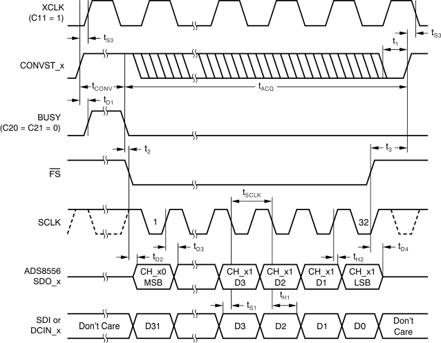
- 6.10 Serial Interface Timing Requirements
- 6.11 Parallel Interface Timing Requirements (Read Access)
- 6.12 Parallel Interface Timing Requirements (Write Access)
- 6.13 Typical Characteristics
- 7 Detailed Description
- 8 Application and Implementation
- 9 Power Supply Recommendations
- 10Layout
- 11Device and Documentation Support
- 12Mechanical, Packaging, and Orderable Information
6 Specifications
6.1 Absolute Maximum Ratings
over operating free-air temperature range (unless otherwise noted)(1)| MIN | MAX | UNIT | |
|---|---|---|---|
| Supply voltage, HVDD to AGND | –0.3 | 18 | V |
| Supply voltage, HVSS to AGND | –18 | 0.3 | V |
| Supply voltage, AVDD to AGND | –0.3 | 6 | V |
| Supply voltage, BVDD to BGND | –0.3 | 6 | V |
| Analog input voltage | HVSS – 0.3 | HVDD + 0.3 | V |
| Reference input voltage with respect to AGND | AGND – 0.3 | AVDD + 0.3 | V |
| Digital input voltage with respect to BGND | BGND – 0.3 | BVDD + 0.3 | V |
| Ground voltage difference AGND to BGND | ±0.3 | V | |
| Input current to all pins except supply | –10 | 10 | mA |
| Maximum virtual junction temperature, TJ | 150 | °C | |
| Storage Temperature, Tstg | -65 | 150 | °C |
(1) Stresses beyond those listed under absolute maximum ratings may cause permanent damage to the device. These are stress ratings only and functional operation of the device at these or any other conditions beyond those indicated under recommended operating conditions is not implied. Exposure to absolute-maximum-rated conditions for extended periods may affect device reliability.
6.2 ESD Ratings
| VALUE | UNIT | |||
|---|---|---|---|---|
| V(ESD) | Electrostatic discharge | Human-body model (HBM), per ANSI/ESDA/JEDEC JS-001 JEDEC standard 22, test method A114-C.01(1) |
±2000 | V |
| Charged-device model (CDM), per JEDEC specification JESD22-C101 JEDEC standard 22, test method C101(2) |
±500 | |||
(1) JEDEC document JEP155 states that 500-V HBM allows safe manufacturing with a standard ESD control process.
(2) JEDEC document JEP157 states that 250-V CDM allows safe manufacturing with a standard ESD control process.
6.3 Recommended Operating Conditions
| MIN | NOM | MAX | UNIT | ||
|---|---|---|---|---|---|
| Supply voltage, AVDD to AGND | 4.5 | 5 | 5.5 | V | |
| Supply voltage, BVDD to BGND | Low-voltage levels | 2.7 | 3.0 | 3.6 | V |
| 5-V logic levels | 4.5 | 5 | 5.5 | ||
| Input supply voltage, HVDD to AGND | Range 1 (±2 × VREF) | 2 × VREF | 16.5 | V | |
| Range 2 (±4 × VREF) | 4 × VREF | 16.5 | |||
| Input supply voltage, HVSS to AGND | Range 1 (±2 × VREF) | –16.5 | –2 × VREF | V | |
| Range 2 (±4 × VREF) | –16.5 | –4 × VREF | |||
| Reference input voltage (VREF) | 0.5 | 2.5 | 3.0 | V | |
| Analog inputs(1) | Range 1 (±2 × VREF) | –2 × VREF | 2 × VREF | V | |
| Range 1 (±4 × VREF) | –4 × VREF | 4 × VREF | |||
| Operating ambient temperature, TA | –40 | 125 | °C | ||
(1) For more information, see the Analog Inputs section.
6.4 Thermal Information
| THERMAL METRIC(1) | ADS855x | UNIT | ||
|---|---|---|---|---|
| PM (LQFP) | ||||
| 64 PINS | ||||
| RθJA | Junction-to-ambient thermal resistance | High-K thermal resistance(2) | 50.3 | °C/W |
| RθJC(top) | Junction-to-case (top) thermal resistance | 12.0 | °C/W | |
| RθJB | Junction-to-board thermal resistance | 24.0 | °C/W | |
| ψJT | Junction-to-top characterization parameter | 0.5 | °C/W | |
| ψJB | Junction-to-board characterization parameter | 23.5 | °C/W | |
| RθJC(bot) | Junction-to-case (bottom) thermal resistance | NA | °C/W | |
(1) For more information about traditional and new thermal metrics, see the Semiconductor and IC Package Thermal Metrics application report, SPRA953.
(2) Modeled in accordance with the Low-K or High-K thermal metric definitions of EIA/JESD51-3.
6.5 Electrical Characteristics: General
over recommended operating free-air temperature range of –40°C to 125°C, AVDD = 4.5 V to 5.5 V, BVDD = 2.7 V to 5.5 V, HVDD = 10 V to 15 V, HVSS = –15 V to –10 V, VREF = 2.5 V (internal), and fDATA = maximum (unless otherwise noted)| PARAMETER | TEST CONDITIONS | MIN | TYP(1) | MAX | UNIT | |
|---|---|---|---|---|---|---|
| ANALOG INPUT | ||||||
| CHXX | Bipolar full-scale range | RANGE pin/RANGE bit = 0 | –4 × VREF | 4 × VREF | V | |
| RANGE pin/RANGE bit = 1 | –2 × VREF | 2 × VREF | ||||
| Input capacitance | Input range = ±4 × VREF | 10 | pF | |||
| Input range = ±2 × VREF | 20 | |||||
| Input leakage current | No ongoing conversion | ±1 | μA | |||
| Aperture delay | 5 | ns | ||||
| Aperture delay matching | Common CONVST for all channels | 250 | ps | |||
| Aperture jitter | 50 | ps | ||||
| EXTERNAL CLOCK INPUT (XCLK) | ||||||
| fXCLK | External clock frequency | An external reference must be used for fXCLK > fCCLK | 1 | 18 | 20 | MHz |
| External clock duty cycle | 45% | 55% | ||||
| REFERENCE VOLTAGE OUTPUT (REFOUT) | ||||||
| VREF | Reference voltage | 2.5-V operation, REFDAC = 0x3FF | 2.485 | 2.5 | 2.515 | V |
| 2.5-V operation, REFDAC = 0x3FF at 25°C | 2.496 | 2.5 | 2.504 | |||
| 3-V operation, REFDAC = 0x3FF | 2.985 | 3.0 | 3.015 | |||
| 3-V operation, REFDAC = 0x3FF at 25°C | 2.995 | 3.0 | 3.005 | |||
| dVREF/dT | Reference voltage drift | ±10 | ppm/°C | |||
| PSRR | Power-supply rejection ratio | 73 | dB | |||
| IREFOUT | Output current | With dc current | –2 | 2 | mA | |
| IREFSC | Short-circuit current(2) | 50 | mA | |||
| tREFON | Turn-on settling time | 10 | ms | |||
| External load capacitance | At CREF_x pins | 4.7 | 10 | μF | ||
| At REFIO pins | 100 | 470 | ||||
| REFDAC | Tuning range | Internal reference output voltage range | 0.2 × VREF | VREF | V | |
| REFDAC resolution | 10 | Bits | ||||
| DNLDAC | REFDAC differential nonlinearity | –1 | ±0.1 | 1 | LSB | |
| INLDAC | REFDAC integral nonlinearity | –2 | ±0.1 | 2 | LSB | |
| VOSDAC | REFDAC offset error | VREF = 0.5 V (DAC = 0x0CC) | –4 | ±0.65 | 4 | LSB |
| REFERENCE VOLTAGE INPUT (REFIN) | ||||||
| VREFIN | Reference input voltage | 0.5 | 2.5 | 3.025 | V | |
| Input resistance | 100 | MΩ | ||||
| Input capacitance | 5 | pF | ||||
| Reference input current | 1 | μA | ||||
| SERIAL CLOCK INPUT (SCLK) | ||||||
| fSCLK | Serial clock input frequency | 0.1 | 36 | MHz | ||
| tSCLK | Serial clock period | 0.0278 | 10 | μs | ||
| Serial clock duty cycle | 40% | 60% | ||||
| DIGITAL INPUTS(3) | ||||||
| Logic family | CMOS with Schmitt-Trigger | |||||
| High-level input voltage | 0.7 × BVDD | BVDD + 0.3 | V | |||
| Low-level input voltage | BGND – 0.3 | 0.3 × BVDD | V | |||
| Input current | VI = BVDD to BGND | –50 | 50 | nA | ||
| Input capacitance | 5 | pF | ||||
| DIGITAL OUTPUTS(3) | ||||||
| Logic family | CMOS | |||||
| High-level output voltage | IOH = 100 μA | BVDD – 0.6 | BVDD | V | ||
| Low-level output voltage | IOH = –100 μA | BGND | BGND + 0.4 | V | ||
| High-impedance-state output current | –50 | 50 | nA | |||
| Output capacitance | 5 | pF | ||||
| Load capacitance | 30 | pF | ||||
| POWER-SUPPLY REQUIREMENTS | ||||||
| AVDD | Analog supply voltage | 4.5 | 5 | 5.5 | V | |
| BVDD | Buffer I/O supply voltage | 2.7 | 3 | 5.5 | V | |
| HVDD | Input positive supply voltage | 5 | 10 | 16.5 | V | |
| HVSS | Input negative supply voltage | –16.5 | –10 | –5 | V | |
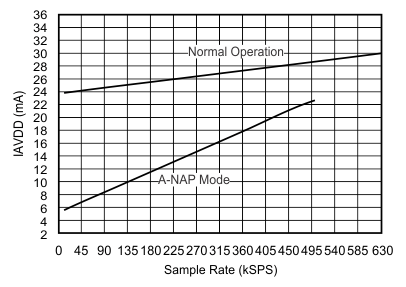
| IAVDD | Analog supply current(4) | fDATA = maximum | 30 | 36 | mA | |
| ADS8556, fDATA = 250 kSPS (auto-NAP mode) | 14 | 16.5 | ||||
| ADS8557, fDATA = 250 kSPS (auto-NAP mode) | 14 | 17 | ||||
| ADS8558, fDATA = 250 kSPS (auto-NAP mode) | 14 | 18 | ||||
| Auto-NAP mode, no ongoing conversion, internal conversion clock | 4 | 6 | ||||
| Power-down mode | 0.1 | 50 | μA | |||
| IBVDD | Buffer I/O supply current(5) | fDATA = maximum | 0.9 | 2 | mA | |
| fDATA = 250 kSPS (auto-NAP mode) | 0.5 | 1.5 | ||||
| Auto-NAP mode, no ongoing conversion, internal conversion clock | 0.1 | 10 | μA | |||
| Power-down mode | 0.1 | 10 | ||||
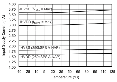
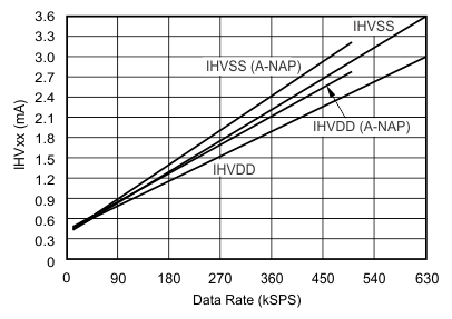
| IHVDD | Input positive supply current(6) | ADS8556, fDATA = maximum | 3 | 3.5 | mA | |
| ADS8557, fDATA = maximum | 3.1 | 3.6 | ||||
| ADS8558, fDATA = maximum | 3.3 | 4 | ||||
| fDATA = 250 kSPS (auto-NAP mode) | 1.6 | 2 | ||||
| Auto-NAP mode, no ongoing conversion, internal conversion clock | 0.2 | 0.3 | μA | |||
| Power-down mode | 0.1 | 10 | ||||
| IHVSS | Input negative supply current(7) | ADS8556, fDATA = maximum | 3.6 | 4 | mA | |
| ADS8557, fDATA = maximum | 3.6 | 4.2 | ||||
| ADS8558, fDATA = maximum | 4 | 4.8 | ||||
| fDATA = 250 kSPS (auto-NAP mode) | 1.8 | 2.2 | ||||
| Auto-NAP mode, no ongoing conversion, internal conversion clock | 0.2 | 0.25 | μA | |||
| Power-down mode | 0.1 | 10 | ||||
| Power dissipation(8) | ADS8556, fDATA = maximum | 251.7 | 298.5 | mW | ||
| ADS8557, fDATA = maximum | 253.2 | 303 | ||||
| ADS8558, fDATA = maximum | 262.2 | 318 | ||||
| ADS8556, fDATA = 250 kSPS (auto-NAP mode) | 122.5 | 150 | ||||
| ADS8557, fDATA = 250 kSPS (auto-NAP mode) | 122.5 | 152.5 | ||||
| ADS8558, fDATA = 250 kSPS (auto-NAP mode) | 122.5 | 157.5 | ||||
| Auto-NAP mode, no ongoing conversion, internal conversion clock | 26 | 38.3 | ||||
| Power-down mode | 3.8 | 580 | μW | |||
(1) All values are at TA = 25°C.
(2) Reference output current is not limited internally.
(3) Specified by design.
(4) At AVDD = 5 V.
(5) At BVDD = 3 V, parallel mode, load capacitance = 6 pF per pin.
(6) At HVDD = 15 V.
(7) At HVSS = –15 V.
(8) At AVDD = 5 V, BVDD = 3 V, HVDD = 15 V, and HVSS = –15 V.
6.6 Electrical Characteristics: ADS8556
over recommended operating free-air temperature range of –40°C to 125°C, AVDD = 4.5 V to 5 V, BVDD = 2.7 V to 5.5 V, HVDD = 10 V to 15 V, HVSS = –15 V to –10 V, VREF = 2.5 V (internal), and fDATA = 630 kSPS in parallel mode or 450 kSPS in serial mode (unless otherwise noted)| PARAMETER | TEST CONDITIONS | MIN | TYP(1) | MAX | UNIT | |
|---|---|---|---|---|---|---|
| DC ACCURACY | ||||||
| Resolution | 16 | Bits | ||||
| No missing codes | 16 | Bits | ||||
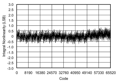
| INL | Integral linearity error | At TA = –40°C to 85°C | –3 | ±1.5 | 3 | LSB |
| At TA = –40°C to 125°C | –4 | ±1.5 | 4 | |||
| DNL | Differential linearity error | At TA = –40°C to 85°C | –1 | ±0.75 | 1.5 | LSB |
| At TA = –40°C to 125°C | –1 | ±0.75 | 2 | |||
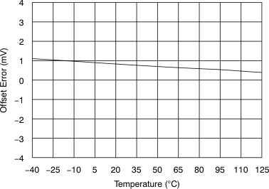
| Offset error | –4 | ±0.8 | 4 | mV | ||
| Offset error drift | ±3.5 | μV/°C | ||||
| Gain error | Referenced to voltage at REFIO | –0.75 | ±0.25 | 0.75 | %FSR | |
| Gain error drift | Referenced to voltage at REFIO | ±6 | ppm/°C | |||
| PSRR | Power-supply rejection ratio | At output code FFFFh, related to AVDD | 60 | dB | ||
| SAMPLING DYNAMICS | ||||||
| tACQ | Acquisition time | 280 | ns | |||
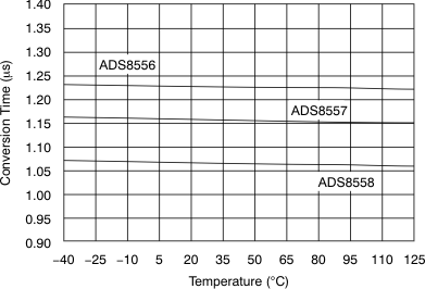
| tCONV | Conversion time per ADC | 1.26 | μs | |||
| tCCLK | Internal conversion clock period | 18.5 | tCCLK | |||
| 68.0 | ns | |||||
| fDATA | Throughput rate | Parallel interface, internal clock and reference | 630 | kSPS | ||
| Serial interface, internal clock and reference | 450 | |||||
| AC ACCURACY | ||||||
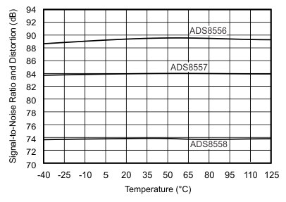
| SNR | Signal-to-noise ratio | At fIN = 10 kHz, TA = –40°C to 85°C | 90 | 91.5 | dB | |
| At fIN = 10 kHz, TA = –40°C to 125°C | 89 | 91.5 | ||||
| SINAD | Signal-to-noise ratio + distortion | At fIN = 10 kHz, TA = –40°C to 85°C | 87 | 89.5 | dB | |
| At fIN = 10 kHz, TA = –40°C to 125°C | 86.5 | 89.5 | ||||
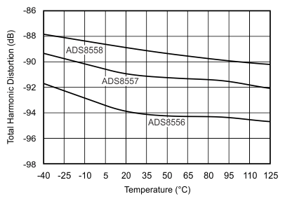
| THD | Total harmonic distortion(2) | At fIN = 10 kHz, TA = –40°C to 85°C | –94 | –90 | dB | |
| At fIN = 10 kHz, TA = –40°C to 125°C | –94 | –89.5 | ||||
| SFDR | Spurious-free dynamic range | At fIN = 10 kHz, TA = –40°C to 85°C | 90 | 95 | dB | |
| At fIN = 10 kHz, TA = –40°C to 125°C | 89.5 | 95 | ||||
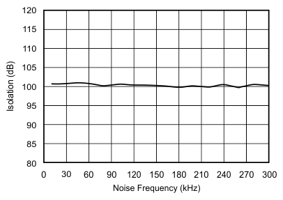
| Channel-to-channel isolation | At fIN = 10 kHz | 100 | dB | |||
| –3-dB small-signal bandwidth | In 4 × VREF mode | 48 | MHz | |||
| In 2 × VREF mode | 24 | |||||
(1) All values are at TA = 25°C.
(2) Calculated on the first nine harmonics of the input frequency.
6.7 Electrical Characteristics: ADS8557
over recommended operating free-air temperature range of –40°C to 125°C, AVDD = 4.5 V to 5.5 V, BVDD = 2.7 V to 5.5 V, HVDD = 10 V to 15 V, HVSS = –15 V to –10 V, VREF = 2.5 V (internal), and fDATA = 670 kSPS in parallel mode or 470 kSPS in serial mode (unless otherwise noted)| PARAMETER | TEST CONDITIONS | MIN | TYP(1) | MAX | UNIT | |
|---|---|---|---|---|---|---|
| DC ACCURACY | ||||||
| Resolution | 14 | Bits | ||||
| No missing codes | 14 | Bits | ||||
| INL | Integral linearity error | –1 | ±0.4 | 1 | LSB | |
| DNL | Differential linearity error | –1 | ±0.25 | 1 | LSB | |
| Offset error | –4 | ±0.8 | 4 | mV | ||
| Offset error drift | ±3.5 | μV/°C | ||||
| Gain error | Referenced to voltage at REFIO | –0.75 | ±0.25 | 0.75 | %FSR | |
| Gain error drift | Referenced to voltage at REFIO | ±6 | ppm/°C | |||
| PSRR | Power-supply rejection ratio | At output code FFFFh, related to AVDD | 60 | dB | ||
| SAMPLING DYNAMICS | ||||||
| tACQ | Acquisition time | 280 | ns | |||
| tCONV | Conversion time per ADC | 1.19 | μs | |||
| tCCLK | Internal conversion clock period | 18.5 | tCCLK | |||
| 64.1 | ns | |||||
| fDATA | Throughput rate | Parallel interface, internal clock and reference | 670 | kSPS | ||
| Serial interface, internal clock and reference | 470 | |||||
| AC ACCURACY | ||||||
| SNR | Signal-to-noise ratio | At fIN = 10 kHz | 84 | 85 | dB | |
| SINAD | Signal-to-noise ratio + distortion | At fIN = 10 kHz | 83 | 84 | dB | |
| THD | Total harmonic distortion(2) | At fIN = 10 kHz | –91 | –86 | dB | |
| SFDR | Spurious-free dynamic range | At fIN = 10 kHz | 86 | 92 | dB | |
| Channel-to-channel isolation | At fIN = 10 kHz | 100 | dB | |||
| –3-dB small-signal bandwidth | In 4 × VREF mode | 48 | MHz | |||
| In 2 × VREF mode | 24 | |||||
(1) All values are at TA = 25°C.
(2) Calculated on the first nine harmonics of the input frequency.
6.8 Electrical Characteristics: ADS8558
over recommended operating free-air temperature range of –40°C to 125°C, AVDD = 4.5 V to 5 V, BVDD = 2.7 V to 5.5 V, HVDD = 10 V to 15 V, HVSS = –15 V to –10 V, VREF = 2.5 V (internal), and fDATA = 730 kSPS in parallel mode or 500 kSPS in serial mode (unless otherwise noted)| PARAMETER | TEST CONDITIONS | MIN | TYP(1) | MAX | UNIT | |
|---|---|---|---|---|---|---|
| DC ACCURACY | ||||||
| Resolution | 12 | Bits | ||||
| No missing codes | 12 | Bits | ||||
| INL | Integral linearity error | –0.75 | ±0.2 | 0.75 | LSB | |
| DNL | Differential linearity error | –0.5 | ±0.2 | 0.5 | LSB | |
| Offset error | –4 | ±0.8 | 4 | mV | ||
| Offset error drift | ±3.5 | μV/°C | ||||
| Gain error | Referenced to voltage at REFIO | –0.75 | ±0.25 | 0.75 | %FSR | |
| Gain error drift | Referenced to voltage at REFIO | ±6 | ppm/°C | |||
| PSRR | Power-supply rejection ratio | At output code FFFFh, related to AVDD | 60 | dB | ||
| SAMPLING DYNAMICS | ||||||
| tACQ | Acquisition time | 280 | ns | |||
| tCONV | Conversion time per ADC | 1.09 | μs | |||
| tCCLK | Internal conversion clock period | 18.5 | tCCLK | |||
| 58.8 | ns | |||||
| fDATA | Throughput rate | Parallel interface, internal clock and reference | 730 | kSPS | ||
| Serial interface, internal clock and reference | 500 | |||||
| AC ACCURACY | ||||||
| SNR | Signal-to-noise ratio | At fIN = 10kHz | 73 | 73.9 | dB | |
| SINAD | Signal-to-noise ratio + distortion | At fIN = 10kHz | 73 | 73.8 | dB | |
| THD | Total harmonic distortion(2) | At fIN = 10kHz | –89 | –84 | dB | |
| SFDR | Spurious-free dynamic range | At fIN = 10kHz | 84 | 92 | dB | |
| Channel-to-channel isolation | At fIN = 10kHz | 100 | dB | |||
| –3-dB small-signal bandwidth | In 4 × VREF mode | 48 | MHz | |||
| In 2 × VREF mode | 24 | |||||
(1) All values are at TA = 25°C.
(2) Calculated on the first nine harmonics of the input frequency.
6.9 Power Dissipation Characteristics
over operating free-air temperature range (unless otherwise noted)6.10 Serial Interface Timing Requirements
over recommended operating free-air temperature range at –40°C to 125°C, AVDD = 5 V, and BVDD = 2.7 V to 5.5 V (unless otherwise noted)(1)(1) All input signals are specified with tR = tF = 1.5 ns (10% to 90% of BVDD) and timed from a voltage level of (VIL + VIH) / 2.
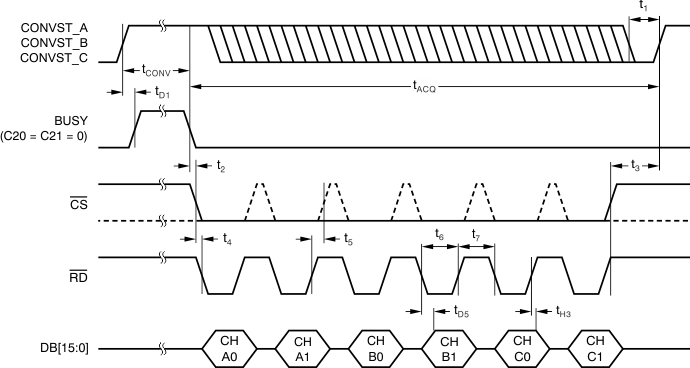
6.11 Parallel Interface Timing Requirements (Read Access)
over recommended operating free-air temperature range at –40°C to 125°C, AVDD = 5 V, and BVDD = 2.7 V to 5.5 V (unless otherwise noted)(1)| MIN | NOM | MAX | UNIT | |||
|---|---|---|---|---|---|---|
| tACQ | Acquisition time | 280 | ns | |||
| tCONV | Conversion time | ADS8556 | 1.26 | µs | ||
| ADS8557 | 1.19 | |||||
| ADS8558 | 1.09 | |||||
| t1 | CONVST_x low time | 20 | ns | |||
| t2 | BUSY low to CS low time | 0 | ns | |||
| t3 | Bus access finished to next conversion start time(2) | ADS8556 | 40 | ns | ||
| ADS8557 | 20 | |||||
| ADS8558 | 0 | |||||
| t4 | CS low to RD low time | 0 | ns | |||
| t5 | RD high to CS high time | 0 | ns | |||
| t6 | RD pulse duration | 30 | ns | |||
| t7 | Minimum time between two read accesses | 10 | ns | |||
| tD1 | CONVST_x high to BUSY high delay | 5 | 20 | ns | ||
| tD5 | RD falling edge to output data valid delay | 20 | ns | |||
| tH3 | Output data to RD rising edge hold time | 5 | ns | |||
(1) All input signals are specified with tR = tF = 1.5 ns (10% to 90% of BVDD) and timed from a voltage level of (VIL + VIH) / 2.
(2) Refer to the CS signal or RD, whichever occurs first.
6.12 Parallel Interface Timing Requirements (Write Access)
over recommended operating free-air temperature range at –40°C to 125°C, AVDD = 5 V, and BVDD = 2.7 V to 5.5 V (unless otherwise noted)(1)| MIN | NOM | MAX | UNIT | ||
|---|---|---|---|---|---|
| t8 | CS low to WR low time | 0 | ns | ||
| t9 | WR low pulse duration | 15 | ns | ||
| t10 | WR high pulse duration | 10 | ns | ||
| t11 | WR high to CS high time | 0 | ns | ||
| tS2 | Output data to WR rising edge setup time | 5 | ns | ||
| tH4 | Data output to WR rising edge hold time | 5 | ns | ||
(1) All input signals are specified with tR = tF = 1.5 ns (10% to 90% of BVDD) and timed from a voltage level of (VIL + VIH) / 2.
 Figure 1. Equivalent Input Circuits
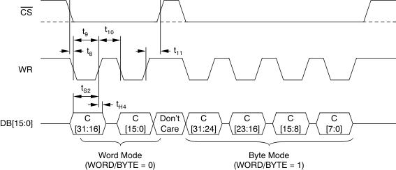 Figure 4. Parallel Write Access Timing Diagram
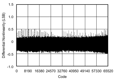
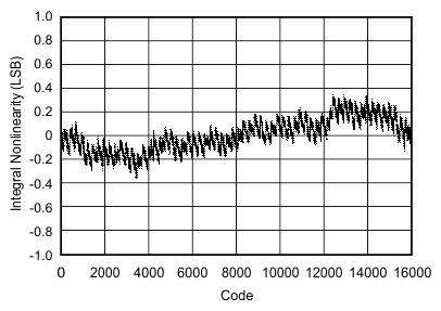
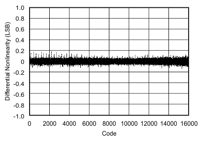
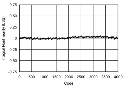
6.13 Typical Characteristics
at 25°C, over entire supply voltage range, VREF = 2.5 V (internal), and fDATA = maximum (unless otherwise noted)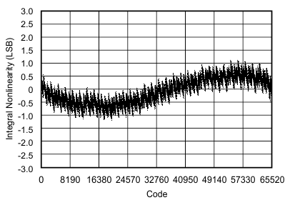
| AVDD = BVDD = 5 V | HVSS = –15 V | HVDD = 15 V |
| fDATA = max | Internal reference |
| AVDD = BVDD = 5 V | HVSS = –15 V | HVDD = 15 V |
| fDATA = max | Internal reference |
| AVDD = BVDD = 5 V | HVSS = –15 V | HVDD = 15 V |
| fDATA = max | Internal reference |
| AVDD = BVDD = 5 V | HVSS = –15 V | HVDD = 15 V |
| fDATA = max | Internal reference |
| AVDD = BVDD = 5 V | HVSS = –15 V | HVDD = 15 V |
| fDATA = max | Internal reference |
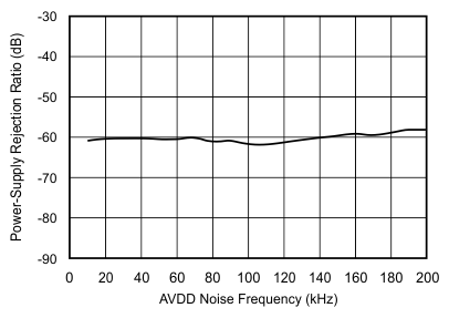
| CSUPPLY = 100 nF on AVDD | ||
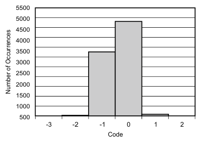
| AVDD = BVDD = 5 V | HVSS = –15 V | HVDD = 15 V |
| Range = 4 × VREF | 8192 samples | Internal reference |
| AVDD = BVDD = 5 V | HVSS = –15 V | HVDD = 15 V |
| Range = ±4 × VREF | fSIGNAL = 10 kHz | fDATA = max |
| Internal reference |
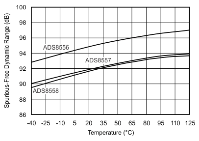
| AVDD = BVDD = 5 V | HVSS = –15 V | HVDD = 15 V |
| Range = ±4 × VREF | fSIGNAL = 10 kHz | fDATA = max |
| Internal reference |
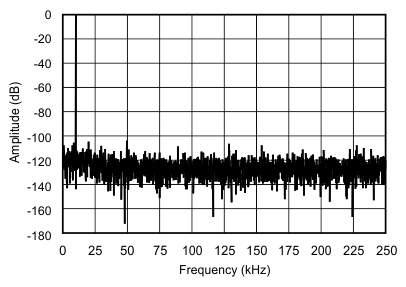
| AVDD = BVDD = 5 V | fSAMPLE = 500 kSPS | HVSS = –15 V |
| Range = ±2 × VREF | fSIGNAL = 10 kHz | HVDD = 15 V |
| Internal reference |
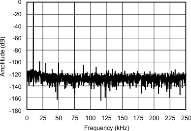
(2048-Point FFT, fIN = 10 kHz, ±5-VIN Range)
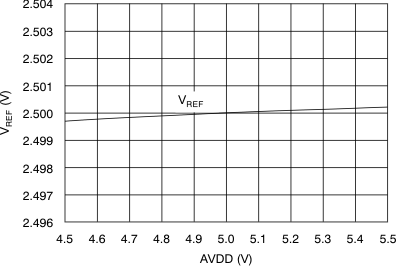
Analog Supply Voltage (2.5-V Mode)
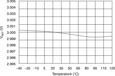
Temperature (3-V Mode)
| AVDD = 5 V | Internal reference |
| Range = ±4 × VREF | HVSS = –15 V | HVDD = 15 V |
| Internal reference |
| Range = ±4 × VREF | HVSS = –15 V | HVDD = 15 V |
| AVDD = BVDD = 5 V | HVSS = –15 V | HVDD = 15 V |
| fDATA = max | Internal reference |

| AVDD = BVDD = 5 V | HVSS = –15 V | HVDD = 15 V |
| fDATA = max | Internal reference |
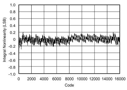
| AVDD = BVDD = 5 V | HVSS = –15 V | HVDD = 15 V |
| fDATA = max | Internal reference |
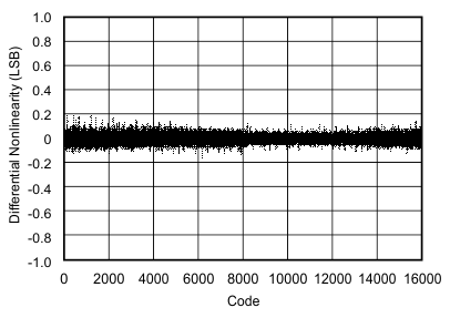
| AVDD = BVDD = 5 V | HVSS = –15 V | HVDD = 15 V |
| fDATA = max | Internal reference |
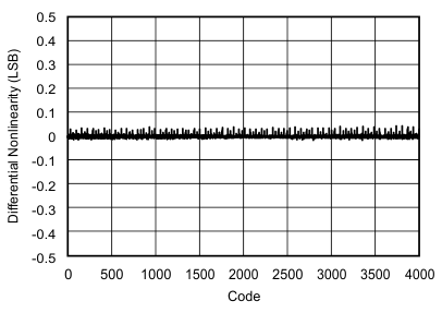
| AVDD = BVDD = 5 V | HVSS = –15 V | HVDD = 15 V |
| fDATA = max | Internal reference |
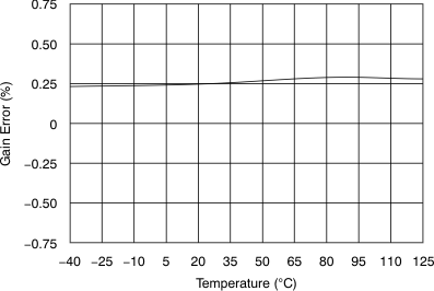

| AVDD = BVDD = 5 V | HVSS = –15 V | HVDD = 15 V |
| Range = ±4 × VREF | fSIGNAL = 10 kHz | fDATA = max |
| Internal reference |
| AVDD = BVDD = 5 V | HVSS = –15 V | HVDD = 15 V |
| Range = ±4 × VREF | fSIGNAL = 10 kHz | fDATA = max |
| Internal reference |
| AVDD = BVDD = 5 V | fSAMPLE = 500 kSPS | HVSS = –15 V |
| Range = ±4 × VREF | fSIGNAL = 10 kHz | HVDD = 15 V |
| Internal reference |
(2048-Point FFT, fIN = 10 kHz, ±10-VIN Range)
| AVDD = BVDD = 5 V | HVSS = –15 V | HVDD = 15 V |
| Range = ±2 × VREF | fDATA = max | Internal reference |
Input Noise Frequency
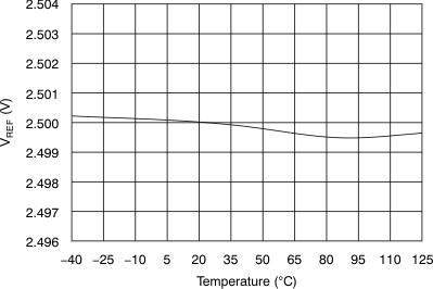
Temperature (2.5-V Mode)
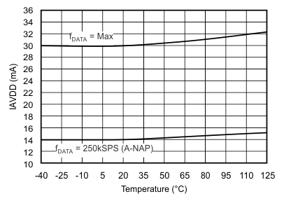
| AVDD = 5 V | Internal reference |
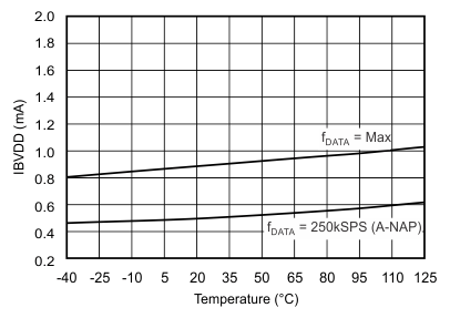
| BVDD = 5 V |
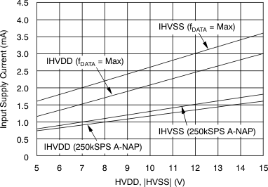
Input Supply Voltage
