ZHCSGU6A september   2017  – july 2023 ADS8588H

PRODUCTION DATA  

  1.   1
  2. 特性
  3. 应用
  4. 说明
  5. Revision History
  6. Pin Configuration and Functions
  7. Specifications
    1. 6.1  Absolute Maximum Ratings
    2. 6.2  ESD Ratings
    3. 6.3  Recommended Operating Conditions
    4. 6.4  Thermal Information
    5. 6.5  Electrical Characteristics
    6. 6.6  Timing Requirements: CONVST Control
    7. 6.7  Timing Requirements: Data Read Operation
    8. 6.8  Timing Requirements: Parallel Data Read Operation, CS and RD Tied Together
    9. 6.9  Timing Requirements: Parallel Data Read Operation, CS and RD Separate
    10. 6.10 Timing Requirements: Serial Data Read Operation
    11. 6.11 Timing Requirements: Byte Mode Data Read Operation
    12. 6.12 Timing Requirements: Oversampling Mode
    13. 6.13 Timing Requirements: Exit Standby Mode
    14. 6.14 Timing Requirements: Exit Shutdown Mode
    15. 6.15 Switching Characteristics: CONVST Control
    16. 6.16 Switching Characteristics: Parallel Data Read Operation, CS and RD Tied Together
    17. 6.17 Switching Characteristics: Parallel Data Read Operation, CS and RD Separate
    18. 6.18 Switching Characteristics: Serial Data Read Operation
    19. 6.19 Switching Characteristics: Byte Mode Data Read Operation
    20. 6.20 Timing Diagrams
    21. 6.21 Typical Characteristics
  8. Detailed Description
    1. 7.1 Overview
    2. 7.2 Functional Block Diagram
    3. 7.3 Feature Description
      1. 7.3.1  Analog Inputs
      2. 7.3.2  Analog Input Impedance
      3. 7.3.3  Input Clamp Protection Circuit
      4. 7.3.4  Programmable Gain Amplifier (PGA)
      5. 7.3.5  Third-Order, Low-Pass Filter (LPF)
      6. 7.3.6  ADC Driver
      7. 7.3.7  Digital Filter and Noise
      8. 7.3.8  Reference
        1. 7.3.8.1 Internal Reference
        2. 7.3.8.2 External Reference
        3. 7.3.8.3 Supplying One VREF to Multiple Devices
      9. 7.3.9  ADC Transfer Function
      10. 7.3.10 ADS8588H Device Family Comparison
    4. 7.4 Device Functional Modes
      1. 7.4.1 Device Interface: Pin Description
        1. 7.4.1.1  REFSEL (Input)
        2. 7.4.1.2  RANGE (Input)
        3. 7.4.1.3  STBY (Input)
        4. 7.4.1.4  PAR/SER/BYTE SEL (Input)
        5. 7.4.1.5  CONVSTA, CONVSTB (Input)
        6. 7.4.1.6  RESET (Input)
        7. 7.4.1.7  RD/SCLK (Input)
        8. 7.4.1.8  CS (Input)
        9. 7.4.1.9  OS[2:0]
        10. 7.4.1.10 BUSY (Output)
        11. 7.4.1.11 FRSTDATA (Output)
        12. 7.4.1.12 DB15/BYTE SEL
        13. 7.4.1.13 DB14/HBEN
        14. 7.4.1.14 DB[13:9]
        15. 7.4.1.15 DB8/DOUTB
        16. 7.4.1.16 DB7/DOUTA
        17. 7.4.1.17 DB[6:0]
      2. 7.4.2 Device Modes of Operation
        1. 7.4.2.1 Power-Down Modes
          1. 7.4.2.1.1 Standby Mode
          2. 7.4.2.1.2 Shutdown Mode
        2. 7.4.2.2 Conversion Control
          1. 7.4.2.2.1 Simultaneous Sampling on All Input Channels
          2. 7.4.2.2.2 Simultaneous Sampling Two Sets of Input Channels
        3. 7.4.2.3 Data Read Operation
          1. 7.4.2.3.1 Parallel Data Read
          2. 7.4.2.3.2 Parallel Byte Data Read
          3. 7.4.2.3.3 Serial Data Read
          4. 7.4.2.3.4 Data Read During Conversion
        4. 7.4.2.4 Oversampling Mode of Operation
  9. Application and Implementation
    1. 8.1 Application Information
    2. 8.2 Typical Application
      1. 8.2.1 Design Requirements
      2. 8.2.2 Detailed Design Procedure
      3. 8.2.3 Application Curve
    3. 8.3 Power Supply Recommendations
    4. 8.4 Layout
      1. 8.4.1 Layout Guidelines
      2. 8.4.2 Layout Examples
  10. Device and Documentation Support
    1. 9.1 Documentation Support
      1. 9.1.1 Related Documentation
    2. 9.2 接收文档更新通知
    3. 9.3 支持资源
    4. 9.4 Trademarks
    5. 9.5 静电放电警告
    6. 9.6 术语表
  11. 10Mechanical, Packaging, and Orderable Information

封装选项

机械数据 (封装 | 引脚)
散热焊盘机械数据 (封装 | 引脚)
订购信息

Oversampling Mode of Operation

The ADS8588H supports the oversampling mode of operation using an on-chip averaging digital filter, as explained in the Digital Filter and Noise section. The device can be configured in oversampling mode by the OS[2:0] pins (see the OS[2:0] section). Figure 7-20 shows a typical timing diagram for the oversampling mode of operation. The input on the OS pins is latched on the falling edge of the BUSY signal to configure the oversampling rate for the next conversion.

GUID-20230516-SS0I-80JP-W2GZ-LF0THWR8FLZF-low.svg Figure 7-20 OSR Mode Operation Timing Diagram

In the oversampling mode of operation, both the CONVSTA and CONVSTB signals must be tied together or driven together. The BUSY signal width varies with the OSR setting because the conversion time increases with increase in OSR, as shown in Figure 7-20. The high time for the BUSY signal increases with the OSR setting, as listed in the Timing Requirements: CONVST ControlTiming Requirements: CONVST Control table.

For any particular OSR setting, the maximum achievable throughput per channel is specified in Table 7-1. If the application is running at a lower throughput, then a higher OSR setting can be selected for further noise reduction and SNR improvement. To maximize the throughput per channel, perform a data read when BUSY is high and a conversion is ongoing in OSR mode. This process enables data read for the previous conversion (see the Data Read During Conversion section). At the falling edge of the BUSY signal, the internal data registers are updated with the new conversion data; thus the read operation must complete and CS must be pulled high for at least tDZ_CSBSY before BUSY goes low (see the Timing Requirements: Data Read OperationTiming Requirements: Data Read OperationTiming Requirements: Data Read Operation table).

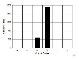
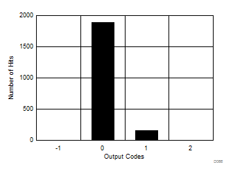
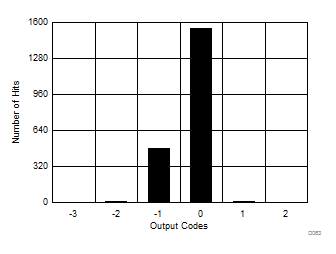
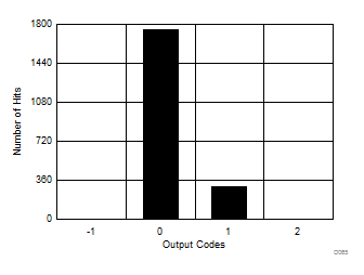
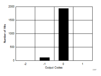
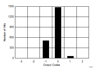
Oversampling the input signal reduces noise during the conversion process, thus reducing the histogram code spread for a dc input signal to the ADC. Figure 7-21 to Figure 7-26 show the effect of oversampling on the output code spread in a dc histogram plot.
GUID-807C4CDC-3EBC-4B3E-B662-0894BE2220B1-low.gif
Mean = –0.22, sigma = 0.48
Figure 7-21 DC Histogram for OSR2
GUID-D1D9D4BB-660F-44E9-8A4B-43CBCDE26C9D-low.gif
Mean = –0.49, sigma = 0.36
Figure 7-23 DC Histogram for OSR8
GUID-4AAFE593-F343-4A16-9B47-8143F88A1DC9-low.gif
Mean = 0.13, sigma = 0.31
Figure 7-25 DC Histogram for OSR32
GUID-B09E1068-EEF0-42ED-A64E-14E3EE202363-low.gif
Mean = –0.43, sigma = 0.41
Figure 7-22 DC Histogram for OSR4
GUID-6DA00B80-CF6A-436D-92F9-C8ED3A1E2CA8-low.gif
Mean = 0.49, sigma = 0.33
Figure 7-24 DC Histogram for OSR16
GUID-8F43F8D3-B5A1-4784-9F31-00C6B35B397B-low.gif
Mean = –0.21, sigma = 0.30
Figure 7-26 DC Histogram for OSR64

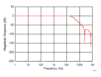
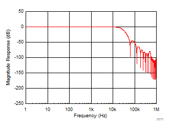
In OSR modes, the device adds a digital filter at the output of the ADC. The digital filter affects the frequency response of the entire data acquisition system including the internal low-pass analog filter and the oversampling digital filter. Figure 7-27 to Figure 7-32 show the frequency response curves for different OSR settings in the ±10-V range.
GUID-7B1591C4-C4BB-421B-91D2-62D0BCE4949B-low.gif
AVDD = 5 V, DVDD = 5 V, TA = 25°C, input range = ±10 V
Figure 7-27 Digital Filter Response for OSR = 2
GUID-26298494-8B3C-4F33-B588-0DE833652CDA-low.gif
AVDD = 5 V, DVDD = 5 V, TA = 25°C, input range = ±10 V
Figure 7-29 Digital Filter Response for OSR = 8
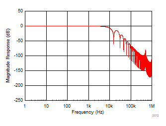
GUID-B3FE94B6-7F21-4D7C-82ED-07B69327661D-low.gif
AVDD = 5 V, DVDD = 5 V, TA = 25°C, input range = ±10 V
Figure 7-31 Digital Filter Response for OSR = 32
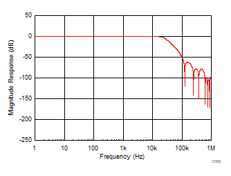
GUID-CA08AFF1-D404-41A9-B15F-93BFEF4F406C-low.gif
AVDD = 5 V, DVDD = 5 V, TA = 25°C, input range = ±10 V
Figure 7-28 Digital Filter Response for OSR = 4
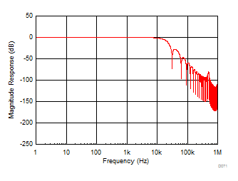
GUID-5877D921-D3EE-44BB-AD27-BC08458955AF-low.gif
AVDD = 5 V, DVDD = 5 V, TA = 25°C, input range = ±10 V
Figure 7-30 Digital Filter Response for OSR = 16
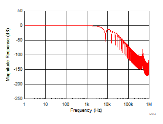
GUID-7BC87033-CD39-46C7-AE9F-AA480298ABC0-low.gif
AVDD = 5 V, DVDD = 5 V, TA = 25°C, input range = ±10 V
Figure 7-32 Digital Filter Response for OSR = 64