ZHCSFT9B December 2016 – March 2021 ADS8671 , ADS8675
PRODUCTION DATA
- 1 特性
- 2 应用
- 3 说明
- 4 Revision History
- 5 Pin Configuration and Functions
-
6 Specifications
- 6.1 Absolute Maximum Ratings
- 6.2 ESD Ratings
- 6.3 Recommended Operating Conditions
- 6.4 Thermal Information
- 6.5 Electrical Characteristics
- 6.6 Timing Requirements: Conversion Cycle
- 6.7 Timing Requirements: Asynchronous Reset
- 6.8 Timing Requirements: SPI-Compatible Serial Interface
- 6.9 Timing Requirements: Source-Synchronous Serial Interface (External Clock)
- 6.10 Timing Requirements: Source-Synchronous Serial Interface (Internal Clock)
- 6.11 Timing Diagrams
- 6.12 Typical Characteristics
-
7 Detailed Description
- 7.1 Overview
- 7.2 Functional Block Diagram
- 7.3 Feature Description
- 7.4 Device Functional Modes
- 7.5 Programming
- 7.6
Register Maps
- 7.6.1
Device Configuration and Register Maps
- 7.6.1.1 DEVICE_ID_REG Register (address = 00h)
- 7.6.1.2 RST_PWRCTL_REG Register (address = 04h)
- 7.6.1.3 SDI_CTL_REG Register (address = 08h)
- 7.6.1.4 SDO_CTL_REG Register (address = 0Ch)
- 7.6.1.5 DATAOUT_CTL_REG Register (address = 10h)
- 7.6.1.6 RANGE_SEL_REG Register (address = 14h)
- 7.6.1.7 ALARM_REG Register (address = 20h)
- 7.6.1.8 ALARM_H_TH_REG Register (address = 24h)
- 7.6.1.9 ALARM_L_TH_REG Register (address = 28h)
- 7.6.1
Device Configuration and Register Maps
- 8 Application and Implementation
- 9 Power Supply Recommendations
- 10Layout
- 11Device and Documentation Support
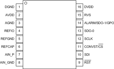
5 Pin Configuration and Functions
 Figure 5-1
PW Package,
16-Pin TSSOP,
Top View (Not to Scale)
Table 5-1 Pin Functions
| NAME | NO. | TYPE(1) | DESCRIPTION |
|---|---|---|---|
| TSSOP | |||
| AGND | 3 | P | Analog ground pin. Decouple with the AVDD pin. |
| AIN_GND | 8 | AI | Analog input: negative. Decouple with the AIN_P pin. |
| AIN_P | 7 | AI | Analog input: positive. Decouple with the AIN_GND pin. |
| ALARM/SDO-1/GPO | 14 | DO | Multi-function output pin. Active high alarm. Data output 1 for serial communication. General-purpose output pin. |
| AVDD | 2 | P | Analog supply pin. Decouple with the AGND pin. |
| CONVST/CS | 11 | DI | Dual-functionality pin. Active high logic: conversion start input pin; a CONVST rising edge brings the device from acquisition phase to conversion phase. Active low logic: chip-select input pin; the device takes control of the data bus when CS is low; the SDO-x pins go to tri-state when CS is high. |
| DGND | 1 | P | Digital ground pin. Decouple with the DVDD pin. |
| DVDD | 16 | P | Digital supply pin. Decouple with the DGND pin. |
| REFCAP | 6 | AO | ADC reference buffer decoupling capacitor pin. Decouple with the REFGND pin. |
| REFGND | 5 | P | Reference ground pin; short to the analog ground plane. Decouple with the REFIO and REFCAP pins. |
| REFIO | 4 | AIO | Internal reference output and external reference input pin. Decouple with REFGND. |
| RST | 9 | DI | Active low logic input to reset the device. |
| RVS | 15 | DO | Multi-function output pin for serial interface; see the Section 7.4.2.1 section. With CS held high, RVS reflects the status of the internal ADCST signal. With CS low, the status of RVS depends on the output protocol selection. |
| SCLK | 12 | DI | Serial communication: clock input pin for the serial interface. All system-synchronous data transfer protocols are timed with respect to the SCLK signal. |
| SDI | 10 | DI | Dual
function: data input pin for serial communication. Chain data input during serial communication in daisy-chain mode. |
| SDO-0 | 13 | DO | Serial communication: data output 0 |
(1) AI = analog input, AIO = analog
input/output, DI = digital input, DO = digital output, and P = power
supply.