SLOS738E September 2012 – August 2015 AFE5809
PRODUCTION DATA.
- 1 Features
- 2 Applications
- 3 Description
- 4 Revision History
- 5 Description (continued)
- 6 Pin Configuration and Functions
-
7 Specifications
- 7.1 Absolute Maximum Ratings
- 7.2 ESD Ratings
- 7.3 Recommended Operating Conditions
- 7.4 Thermal Information
- 7.5 Electrical Characteristics
- 7.6 Digital Demodulator Electrical Characteristics
- 7.7 Digital Characteristics
- 7.8 Switching Characteristics
- 7.9 SPI Switching Characteristics
- 7.10 Output Interface Timing Requirements (14-bit)
- 7.11 Typical Characteristics
-
8 Detailed Description
- 8.1 Overview
- 8.2 Functional Block Diagram
- 8.3 Feature Description
- 8.4 Device Functional Modes
- 8.5 Programming
- 8.6
Register Maps
- 8.6.1
ADC and VCA Register Description
- 8.6.1.1 ADC Register Map
- 8.6.1.2
AFE5809 ADC Register/Digital Processing Description
- 8.6.1.2.1 AVERAGING_ENABLE: Address: 2[11]
- 8.6.1.2.2 ADC_OUTPUT_FORMAT: Address: 4[3]
- 8.6.1.2.3 ADC Reference Mode: Address 1[13] and 3[15]
- 8.6.1.2.4 DIGITAL_GAIN_ENABLE: Address: 3[12]
- 8.6.1.2.5 DIGITAL_HPF_ENABLE
- 8.6.1.2.6 DIGITAL_HPF_FILTER_K_CHX
- 8.6.1.2.7 LOW_FREQUENCY_NOISE_SUPPRESSION: Address: 1[11]
- 8.6.1.2.8 LVDS_OUTPUT_RATE_2X: Address: 1[14]
- 8.6.1.2.9 CHANNEL_OFFSET_SUBSTRACTION_ENABLE: Address: 3[8]
- 8.6.1.2.10 SERIALIZED_DATA_RATE: Address: 3[14:13]
- 8.6.1.2.11 TEST_PATTERN_MODES: Address: 2[15:13]
- 8.6.1.2.12 SYNC_PATTERN: Address: 10[8]
- 8.6.1.3 VCA Register Map
- 8.6.1.4 VCA Register Description
- 8.6.2 Digital Demodulator Register Description
- 8.6.1
ADC and VCA Register Description
-
9 Application and Implementation
- 9.1 Application Information
- 9.2 Typical Application
- 9.3 System Example
- 9.4
Do's and Don'ts
- 9.4.1 Driving the Inputs (Analog or Digital) Beyond the Power-Supply Rails
- 9.4.2 Driving the Device Signal Input With an Excessively High Level Signal
- 9.4.3 Driving the VCNTL Signal With an Excessive Noise Source
- 9.4.4 Using a Clock Source With Excessive Jitter, an Excessively Long Input Clock Signal Trace, or Having Other Signals Coupled to the ADC or CW Clock Signal Trace
- 9.4.5 LVDS Routing Length Mismatch
- 9.4.6 Failure to Provide Adequate Heat Removal
- 10Power Supply Recommendations
- 11Layout
- 12Device and Documentation Support
- 13Mechanical, Packaging, and Orderable Information
8 Detailed Description
8.1 Overview
The AFE5809 device is a highly-integrated AFE solution specifically designed for ultrasound systems in which high performance and small size are required. The AFE5809 device integrates a complete TGC imaging path and a CWD path. It also enables users to select one of various power/noise combinations to optimize system performance. The AFE5809 device contains eight channels; each channel includes a LNA, VCAT, PGA, LPF, 14-bit ADC, digital I/Q demodulator, and CW mixer.
Multiple features in the AFE5809 device are suitable for ultrasound applications, such as active termination, individual channel control, fast power-up and power-down response, programmable clamp voltage control, and fast and consistent overload recovery. Therefore, the AFE5809 device brings premium image quality to ultraportable, handheld systems all the way up to high-end ultrasound systems.
In addition, the signal chain of the AFE5809 device can handle signal frequency as low as 50 kHz and as high as 30 MHz. This enables the AFE5809 device to be used in both sonar and medical applications.
Figure 60 shows a simplified functional block diagram.
8.2 Functional Block Diagram
 Figure 60. Simplified Functional Block Diagram
8.3 Feature Description
8.3.1 LNA
In many high-gain systems, a LNA is critical to achieve overall performance. Using a new proprietary architecture, the LNA in the AFE5809 device delivers exceptional low-noise performance, while operating on a low-quiescent current compared to CMOS-based architectures with similar noise performance. The LNA performs single-ended input to differential output voltage conversion. It is configurable for a programmable gain of 24, 18, or 12 dB and its input-referred noise is only 0.63, 0.7, or 0.9 nV/√Hz, respectively. Programmable gain settings result in a flexible linear input range up to 1 Vpp, realizing high-signal handling capability demanded by new transducer technologies. A larger input signal can be accepted by the LNA; however, the signal can be distorted because it exceeds the LNA’s linear operation region. Combining the low noise and high-input range, the device consequently achieves a wide-input dynamic range for supporting the high demands from various ultrasound imaging modes.
The LNA input is internally biased at approximately 2.4 V; the signal source should be AC-coupled to the LNA input by an adequately-sized capacitor, for example ≥0.1 µF. To achieve low DC offset drift, the AFE5809 device incorporates a DC offset correction circuit for each amplifier stage. To improve the overload recovery, an integrator circuit is used to extract the DC component of the LNA output and then fed back to the LNA’s complementary input for DC offset correction. This DC offset correction circuit has a high-pass response and can be treated as a HPF. The effective corner frequency is determined by the capacitor CBYPASS connected at INM. With larger capacitors, the corner frequency is lower. For stable operation at the highest HP filter cut-off frequency, a ≥15-nF capacitor can be selected. This corner frequency scales almost linearly with the value of the CBYPASS. For example, 15 nF gives a corner frequency of approximately 100 kHz, while 47 nF can give an effective corner frequency of 33 kHz. The DC offset correction circuit can also be disabled or enabled through register 52[12]. A large capacitor like 1 µF can be used for setting low corner frequency (<2 kHz) of the LNA DC offset correction circuit. Figure 59 shows the frequency responses for low-frequency applications.
The AFE5809 device can be terminated passively or actively. Active termination is preferred in ultrasound applications for reducing reflection from mismatches and achieving better axial resolution without degrading noise figure too much. Active termination values can be preset to 50, 100, 200, and 400 Ω; other values also can be programmed by users through register 52[4:0]. A feedback capacitor is required between ACTx and the signal source as Figure 62 shows. On the active termination path, a clamping circuit is also used to create a low-impedance path when overload signal is seen by the AFE5809 device. The clamp circuit limits large input signals at the LNA inputs and improves the overload recovery performance of the AFE5809 device. The clamp level can be set to 350 mVpp, 600 mVpp, or 1.15 Vpp automatically depending on the LNA gain settings when register 52[10:9] = 0. Other clamp voltages, such as 1.15 Vpp, 0.6 Vpp, and 1.5 Vpp, are also achievable by setting register 52[10:9]. This clamping circuit is also designed to obtain good pulse inversion performance and reduce the impact from asymmetric inputs.
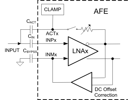 Figure 62. AFE5809 LNA With DC Offset Correction Circuit
8.3.2 Voltage-Controlled Attenuator
The voltage-controlled attenuator is designed to have a linear-in-dB attenuation characteristic; that is, the average gain loss in dB (refer to Figure 2) is constant for each equal increment of the control voltage (VCNTL) as shown in Figure 63. A differential control structure is used to reduce common mode noise. Figure 63 and Figure 64 show a simplified attenuator structure.
The attenuator is essentially a variable voltage divider that consists of the series input resistor (RS) and seven shunt FETs placed in parallel and controlled by sequentially activated clipping amplifiers (A1 through A7). VCNTL is the effective difference between VCNTLP and VCNTLM. Each clipping amplifier can be understood as a specialized voltage comparator with a soft transfer characteristic and well-controlled output limit voltage. Reference voltages V1 through V7 are equally spaced over the 0- to 1.5-V control voltage range. As the control voltage increases through the input range of each clipping amplifier, the amplifier output rises from a voltage where the FET is nearly OFF to VHIGH where the FET is completely ON. As each FET approaches its ON state and the control voltage continues to rise, the next clipping amplifier/FET combination takes over for the next portion of the piecewise-linear attenuation characteristic. Thus, low control voltages have most of the FETs turned OFF, producing minimum signal attenuation. Similarly, high control voltages turn the FETs ON, leading to maximum signal attenuation. Therefore, each FET acts to decrease the shunt resistance of the voltage divider formed by RS and the parallel FET network.
Additionally, a digitally-controlled TGC mode is implemented to achieve better phase-noise performance in the AFE5809 device. The attenuator can be controlled digitally instead of the analog control voltage, VCNTL. This mode can be set by the register bit 59[7]. The variable voltage divider is implemented as a fixed series resistance and FET as the shunt resistance. Each FET can be turned on by connecting the switches SW1 through SW7. Turning on each of the switches can give approximately 6 dB of attenuation. This can be controlled by the register bits 59[6:4]. This digital control feature can eliminate the noise from the VCNTL circuit and ensure better SNR and phase noise for the TGC path.
 Figure 63. Simplified Voltage-Controlled Attenuator (Analog Structure)
 Figure 64. Simplified Voltage-Controlled Attenuator (Digital Structure)
The voltage-controlled attenuator’s noise follows a monotonic relationship to the attenuation coefficient. At higher attenuation, the input-referred noise is higher and vice-versa. The attenuator’s noise is then amplified by the PGA and becomes the noise floor at ADC input. In the attenuator’s high-attenuation operating range, that is VCNTL is high, the attenuator’s input noise may exceed the LNA output noise; the attenuator then becomes the dominant noise source for the following PGA stage and ADC. Therefore, the attenuator noise should be minimized compared to the LNA output noise. The AFE5809 attenuator is designed for achieving very-low noise even at high attenuation (low channel gain) and realizing better SNR in near field. Table 1 lists the input referred noise for different attenuations.
Table 1. Voltage-Controlled-Attenuator Noise versus Attenuation
| ATTENUATION (dB) | ATTENUATOR INPUT REFERRED NOISE (nV/rtHz) |
|---|---|
| –40 | 10.5 |
| –36 | 10 |
| –30 | 9 |
| –24 | 8.5 |
| –18 | 6 |
| –12 | 4 |
| –6 | 3 |
| 0 | 2 |
8.3.3 PGA
After the voltage-controlled attenuator, a PGA can be configured as 24 or 30 dB with a constant-input referred noise of 1.75 nV/rtHz. The PGA structure consists of a differential voltage-to-current converter with programmable gain, clamping circuits, a transimpedance amplifier with a programmable LPF, and a DC offset correction circuit. Figure 65 shows its simplified block diagram.
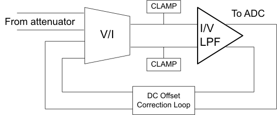 Figure 65. Simplified Block Diagram of PGA
Low input noise is always preferred in a PGA, and its noise contribution should not degrade the ADC SNR too much after the attenuator. At the minimum attenuation (used for small input signals), the LNA noise dominates; at the maximum attenuation (large input signals), the PGA and ADC noise dominates. Thus, 24-dB gain of PGA achieves better SNR as long as the amplified signals can exceed the noise floor of the ADC.
The PGA clamping circuit can be enabled (register 51) to improve the overload recovery performance of the AFE. If the user measures the standard deviation of the output just after overload, for 0.5 V VCNTL, it is about 3.2 LSBs in normal case, that is, the output is stable in about 1 clock cycle after overload. With the clamp disabled, the value approaches 4 LSBs meaning a longer time duration before the output stabilizes; however, with the clamp enabled, there will be degradation in HD3 for PGA output levels >–2 dBFS. For example, for a –2-dBFS output level, the HD3 degrades by approximately 3 dB. To maximize the output dynamic range, the maximum PGA output level can be above 2 Vpp even with the clamp circuit enabled; the ADC in the AFE5809 device has excellent overload recovery performance to detect small signals right after the overload.
NOTE
In the low-power and medium-power modes, PGA_CLAMP is disabled for saving power if 51[7] = 0.
The AFE5809 device integrates an anti-aliasing filter in the form of a programmable LPF in the transimpedance amplifier. The LPF is designed as a differential, active, third-order filter with Butterworth characteristics and a typical 18 dB per octave roll-off. Programmable through the serial interface, the –1-dB frequency corner can be set to one of 10, 15, 20, and 30 MHz. The filter bandwidth is set for all channels simultaneously.
A selectable DC offset correction circuit is implemented in the PGA as well. This correction circuit is similar to the one used in the LNA. It extracts the DC component of the PGA outputs and feeds back to the PGA complementary inputs for DC offset correction. This DC offset correction circuit also has a high-pass response with a cut-off frequency of 80 kHz.
8.3.4 ADC
The ADC of the AFE5809 device employs a pipelined converter architecture that consists of a combination of multi-bit and single-bit internal stages. Each stage feeds its data into the digital error correction logic, ensuring excellent differential linearity and no missing codes at the 14-bit level. The 14 bits given out by each channel are serialized and sent out on a single pair of pins in LVDS format. All eight channels of the AFE5809 device operate from a common input clock (CLKP/M). The sampling clocks for each of the eight channels are generated from the input clock using a carefully matched clock buffer tree. The 14× clock required for the serializer is generated internally from the CLKP/M pins. A 7× and 1× clock are also given out in LVDS format, along with the data, to enable easy data capture. The AFE5809 device operates from internally-generated reference voltages that are trimmed to improve the gain matching across devices. The nominal values of REFP and REFM are 1.5 and 0.5 V, respectively. Alternatively, the device also supports an external reference mode that can be enabled using the serial interface.
Using serialized LVDS transmission has multiple advantages, such as a reduced number of output pins (saving routing space on the board), reduced power consumption, and reduced effects of digital-noise coupling to the analog circuit inside the AFE5809 device.
8.3.5 Continuous-Wave (CW) Beamformer
CWD is a key function in mid-end to high-end ultrasound systems. Compared to the TGC mode, the CW path needs to handle high dynamic range along with strict phase-noise performance. CW beamforming is often implemented in analog domain due to the strict requirements. Multiple beamforming methods are implemented in ultrasound systems, including passive delay line, active mixer, and passive mixer. Among all of them, the passive mixer approach achieves optimized power and noise. It satisfies the CW processing requirements, such as wide dynamic range, low phase noise, accurate gain and phase matching.
Figure 66 and Figure 67 show a simplified CW path block diagram and an in-phase or quadrature (I/Q) channel block diagram, respectively. Each CW channel includes a LNA, a voltage-to-current converter, a switch-based mixer, a shared summing amplifier with a LPF, and clocking circuits.
NOTE
The local oscillator inputs of the passive mixer are cos(ωt) for I-CH and sin(ωt) for Q-CH respectively. Depending on the users' CW Doppler complex FFT processing, swapping I/Q channels in FPGA or DSP may be needed to get correct blood flow directions.
All blocks include well-matched in-phase and quadrature channels to achieve good image frequency rejection as well as beamforming accuracy. As a result, the image rejection ratio from an I/Q channel is better than –46 dBc, which is desired in ultrasound systems.
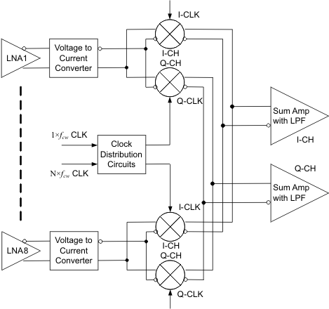 Figure 66. Simplified Block Diagram of CW Path
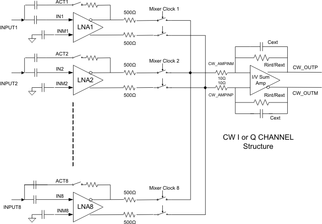
The CW mixer in the AFE5809 device is passive and switch based; a passive mixer adds less noise than an active mixer. It achieves good performance at low power. Figure 68 and the equations describe the principles of mixer operation, where Vi(t), Vo(t), and LO(t) are input, output, and local oscillator (LO) signals for a mixer respectively. The LO(t) is square-wave based and includes odd harmonic components, as shown in Equation 1.
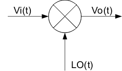 Figure 68. Block Diagram of Mixer Operation
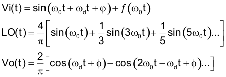
From Equation 1, the third-order and fifth-order harmonics from the LO can interface with the third-order and fifth-order harmonic signals in the Vi(t), or the noise around the third-order and fifth-order harmonics in the Vi(t). Therefore, the mixer’s performance is degraded. To eliminate this side effect due to the square-wave demodulation, a proprietary harmonic-suppression circuit is implemented in the AFE5809 device. The third- and fifth-harmonic components from the LO can be suppressed by over 12 dB. Thus, the LNA output noise around the third-order and fifth-order harmonic bands is not down-converted to base band. Hence, the device achieves better noise figure. The conversion loss of the mixer is about –4 dB, which is derived from  .
.
The mixed current outputs of the eight channels are summed together internally. An internal low-noise operational amplifier is used to convert the summed current to a voltage output. The internal summing amplifier is designed to accomplish low-power consumption, low noise, and ease of use. CW outputs from multiple AFE5809 devices can be further combined on system board to implement a CW beamformer with more than eight channels. See Typical Application for more detailed information.
Multiple clock options are supported in the AFE5809 CW path. Two CW clock inputs are required: N × ƒcw clock and 1 × ƒcw clock, where ƒcw is the CW transmitting frequency and N could be 16, 8, 4, or 1. Users have the flexibility to select the most convenient system clock solution for the AFE5809 device. In the 16 × ƒcw and 8 × ƒcw modes, the third- and fifth-harmonic suppression feature can be supported. Thus, the 16 × ƒcw and 8 × ƒcw modes achieve better performance than the 4 × ƒcw and 1 × ƒcw modes.
8.3.5.1 16 × ƒcw Mode
The 16 × ƒcw mode achieves the best phase accuracy compared to other modes. It is the default mode for CW operation. In this mode, 16 × ƒcw and 1 × ƒcw clocks are required. 16 × ƒcw generates LO signals with 16 accurate phases. Multiple AFE5809 devices can be synchronized by the 1 × ƒcw , that is LO signals in multiple AFEs can have the same starting phase. The phase noise specification is critical only for 16× clock. The 1× clock is for synchronization only and does not require low phase noise. See the phase noise requirement in Typical Application.
Figure 69 shows the top-level clock distribution diagram. Each mixer's clock is distributed through a 16 × 8 cross-point switch. The inputs of the cross-point switch are 16 different phases of the 1× clock. TI recommends aligning the rising edges of the 1 × ƒcw and 16 × ƒcw clocks.
The cross-point switch distributes the clocks with appropriate phase delay to each mixer. For example, Vi(t) is a received signal with a delay of  , a delayed LO(t) should be applied to the mixer to compensate for the
  delay. Thus a 22.5⁰ delayed clock, that is
  , is selected for this channel. The mathematic calculation is expressed in the following equations:
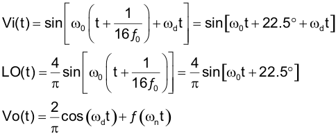
Vo(t) represents the demodulated Doppler signal of each channel. When the Doppler signals from N channels are summed, the signal-to-noise ratio improves.
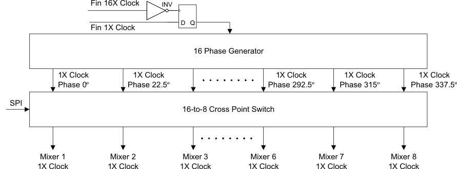 Figure 69.
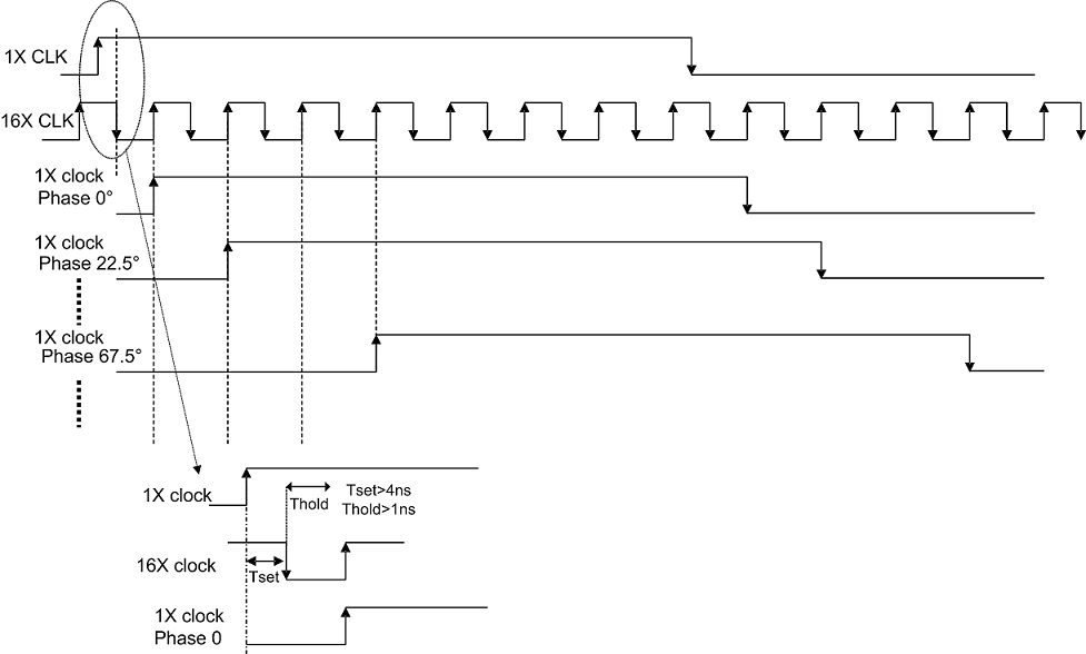 Figure 70. 1× and 16× CW Clock Timing
8.3.5.2 8 × ƒcw and 4 × ƒcw Modes
8 × ƒcw and 4 × ƒcw modes are alternative modes when a higher frequency clock solution (that is 16 × ƒcw clock) is not available in system. Figure 71 shows a block diagram of these two modes.
Good phase accuracy and matching are also maintained. Quadrature clock generator is used to create in-phase and quadrature clocks with exactly 90° phase difference. The only difference between 8 × ƒcw and 4 × ƒcw modes is the accessibility of the third- and fifth-harmonic suppression filter. In the 8 × ƒcw mode, the suppression filter can be supported. In both modes,  phase delay resolution is achieved by weighting the in-phase and quadrature paths correspondingly. For example, if a delay of
  or 22.5° is targeted, the weighting coefficients should follow Equation 3, assuming Iin and Qin are sin(ω0t) and cos(ω0t) respectively.

Therefore, after I/Q mixers, phase delay in the received signals is compensated. The mixers’ outputs from all channels are aligned and added linearly to improve the signal-to-noise ratio. It is preferred to have the 4 × ƒcw or 8 × ƒcw and 1 × ƒcw clocks both aligned at the rising edge.
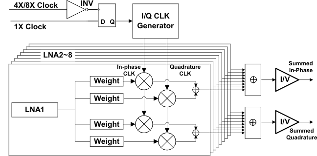 Figure 71. 8 × ƒcw and 4 × ƒcw Block Diagram
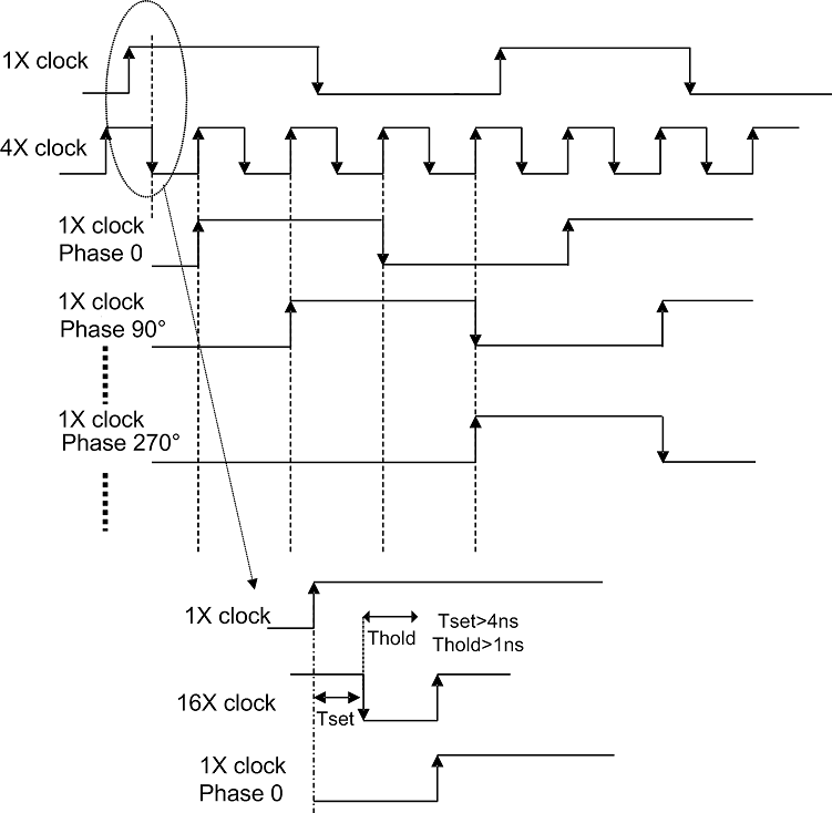 Figure 72. 8 × ƒcw and 4 × ƒcw Timing Diagram
8.3.5.3 1 × ƒcw Mode
The 1 × ƒcw mode requires in-phase and quadrature clocks with low phase noise specifications. The  phase delay resolution is also achieved by weighting the in-phase and quadrature signals as described in the 8 × ƒcw and 4 × ƒcw modes.
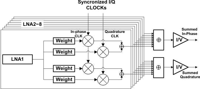 Figure 73. Block Diagram of 1 x ƒcw mode
8.3.6 Digital I/Q Demodulator
The AFE5809 device also includes a digital in-phase and quadrature (I/Q) demodulator and a low-pass decimation filter. The main purpose of the demodulation block is to reduce the LVDS data rate and improve overall system power efficiency. The I/Q demodulator accepts ADC output with up to 65-MSPS sampling rate and 14-bit resolution. For example, after digital demodulation and 4× decimation filtering, the data rate for either in-phase or quadrature output is reduced to 16.25 MSPS, and the data resolution is improved to 16 bits consequently. Hence, the overall LVDS trace reduction can be a factor of 2. This demodulator can be bypassed and powered down completely if it is not needed.
The digital demodulator block given in the AFE5809 device is designed to do down-conversion followed by decimation. The top-level block is divided into two exactly similar blocks: (1) subchip0 and (2) subchip1. Both subchips share four channels each, that is, subchip0 (ADC.1, ADC.2, ADC.3, and ADC.4) and subchip1 (ADC.5, ADC.6, ADC.7, and ADC.8).
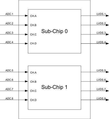 Figure 74. Subchip
The following four functioning blocks are given in each demodulator. Every block can be bypassed.
- DC removal block
- Down conversion
- Decimator
- Channel multiplexing
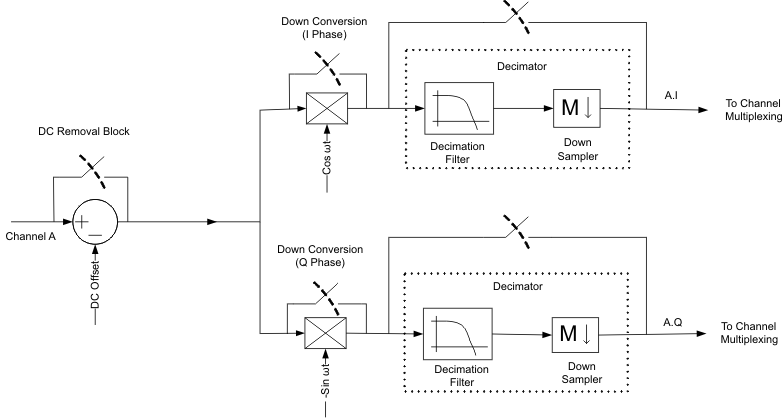 Figure 75. Digital Demodulator Block
- DC removal block is used to remove DC offset. An offset value can be given to a specific register.
- Down conversion or demodulation of signal is done by multiplying signal by cos(ω0t) and by –sin(ω0t) to give out I phase and Q phase, respectively. cos(ωt) and –sin(ωt) are 14-bit wide plus a sign bit. ω = 2πƒ, ƒ can be set with resolution Fs / 216, where Fs is the ADC sampling frequency.
- The decimator block has two functions: decimation filter and down sampler. Decimation filter is a variable coefficient symmetric FIR filter and its coefficients can be given using coefficient RAM. Number of taps of FIR filter is 16× decimation factor (M). For decimation factor of M, 8M coefficients must be stored in the coefficient bank. Each coefficient is 14-bit wide. Down-sampler gives out 1 sample followed by M – 1 samples zeros.
- In Figure 76, channel multiplexing is implemented for flexible data routing:
NOTE
The digital demodulator is based on a conventional down converter, that is, –sin(ω0t) is used for Q phase.
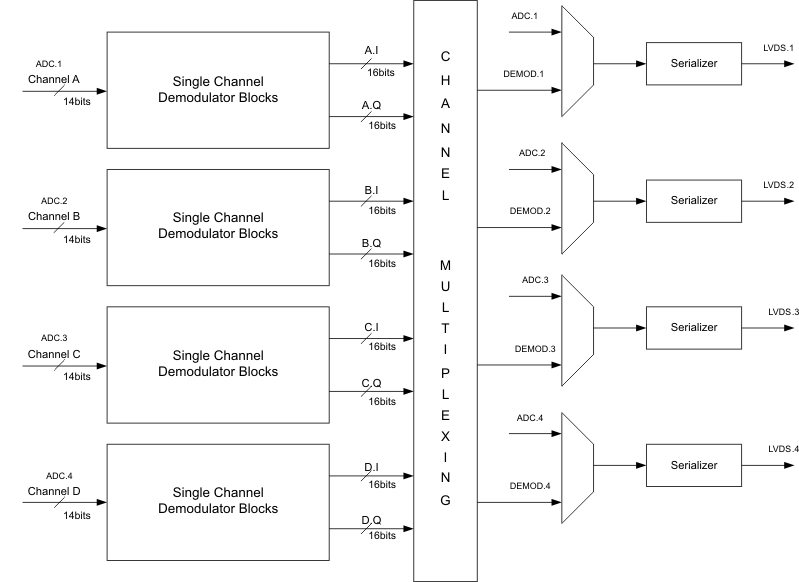 Figure 76. Channel Multiplexing
8.3.7 Equivalent Circuits
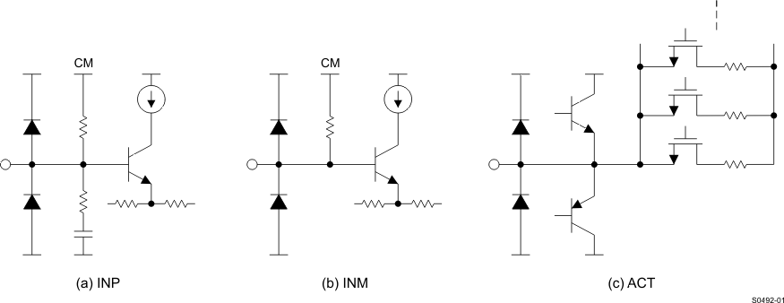 Figure 77. Equivalent Circuits of LNA Inputs
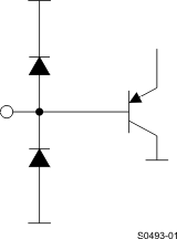 Figure 78. Equivalent Circuits of VCNTLP/M
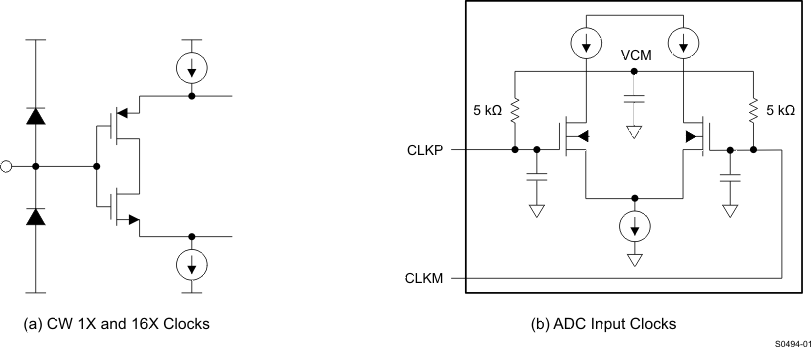 Figure 79. Equivalent Circuits of Clock Inputs
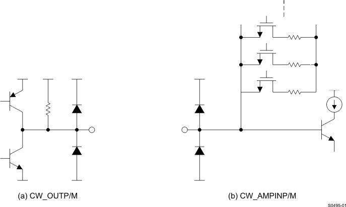 Figure 80. Equivalent Circuits of CW Summing Amplifier Inputs and Outputs
 Figure 81. Equivalent Circuits of LVDS Outputs
8.3.8 LVDS Output Interface Description
The AFE5809 device has a LVDS output interface, which supports multiple output formats. The ADC resolutions can be configured as 12 bit or 14 bit as shown in the LVDS timing diagrams (Figure 1). The ADCs in the AFE5809 device are running at 14 bits; 2 LSBs are removed when 12-bit output is selected; and two zeros are added at LSBs when 16-bit output is selected. Appropriate ADC resolutions can be selected for optimizing system-performance cost effectiveness. When the devices run at 16-bit mode, higher-end FPGAs are required to process the higher rate of LVDS data. Corresponding register settings are listed in Table 4.
8.4 Device Functional Modes
The AFE5809 device is a highly-integrated AFE solution. The AFE5809 device has two functional modes: pulsed-wave imaging mode and continous-wave Doppler imaging mode. When the AFE5809 device operates in the pulsed-wave imaging mode, LNA, VCAT, PGA, LPF, 14-bit ADC, and digital I/Q demodulator are active. In the CWD imaging mode, only LNA and CW mixer are enabled. Either mode can be enabled or programmed by the registers described below.
8.5 Programming
8.5.1 Serial Peripheral Interface (SPI) Operation
The AFE5809 device has two SPIs. The demodulator SPI interface is independent from the ADC/VCA SPI as shown in Figure 82. SPI_DIG_EN is used to select ADC/VCA SPI (SPI_DIG_EN='1') or demod SPI (SPI_DIG_EN='0').
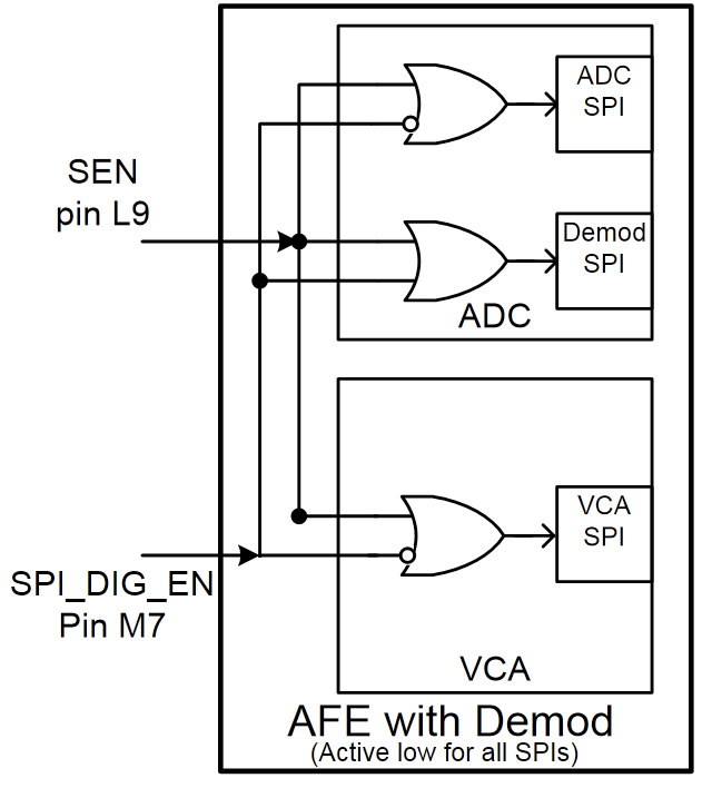 Figure 82. SPI Interface in the AFE5809 Device
8.5.1.1 ADC/VCA Serial Register Write Description
Programming of different modes can be done through the serial interface formed by pins SEN (serial interface enable), SCLK (serial interface clock), SDATA (serial interface data), and RESET. All these pins have a pulldown resistor to GND of 20 kΩ. Serial shift of bits into the device is enabled when SEN is low. Serial data, SDATA, is latched at every rising edge of SCLK when SEN is active (low). The serial data is loaded into the register at every 24th SCLK rising edge when SEN is low. If the word length exceeds a multiple of 24 bits, the excess bits are ignored. Data can be loaded in multiple of 24-bit words within a single active SEN pulse (an internal counter counts groups of 24 clocks after the falling edge of SEN). The interface can work with the SCLK frequency from 20 MHz to low speeds (of a few Hertz) and even with non-50% duty cycle SCLK. The data is divided into two main portions: a register address (8 bits) and the data itself (16 bits), to load on the addressed register. When writing to a register with unused bits, set these to 0. Figure 83 shows this process.
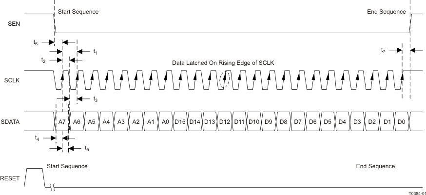 Figure 83. SPI Timing
NOTE
TI recommends synchronizing SCLK to ADC CLK. Typically, SCLK can be generated by dividing ADC CLK by an integer factor of N. In a system with multiple AFEs, SCLKs may not reach all AFEs simultaneously due to routing. To compensate routing differences and ensure AFEs’ outputs are aligned, SCLK can be adjusted to toggle on either the falling edge of ADCLK or the rising edge of ADC CLK (ensuring new register settings are loaded before next ADC sampling clock).
8.5.1.2 ADC/VCA Serial Register Readout Description
The device includes an option where the contents of the internal registers can be read back. This may be useful as a diagnostic test to verify the serial interface communication between the external controller and the AFE. First, the <REGISTER READOUT ENABLE> bit (Reg0[1]) needs to be set to 1. Then, the user should initiate a serial interface cycle specifying the address of the register (A7 through A0) whose content must be read. The data bits are don’t care. The device outputs the contents (D15 through D0) of the selected register on the SDOUT pin. SDOUT has a typical delay, t8, of 20 ns from the falling edge of the SCLK. For lower speed SCLK, SDOUT can be latched on the rising edge of SCLK. For higher speed SCLK, for example, if the SCLK period is less than 60 ns, it is better to latch the SDOUT at the next falling edge of SCLK. Figure 84 shows this operation (the timing specifications follow the same information provided). In the readout mode, users still can access the <REGISTER READOUT ENABLE> through SDATA/SCLK/SEN. To enable serial register writes, set the <REGISTER READOUT ENABLE> bit back to 0.
The AFE5809 SDOUT buffer is tri-stated and gets enabled only when 0[1] (REGISTER READOUT ENABLE) is enabled. SDOUT pins from multiple AFE5809 devices can be tied together without any pullup resistors. Level shifter SN74AUP1T04 can be used to convert 1.8-V logic to 2.5-V/3.3-V logics if needed.
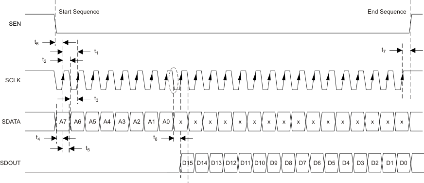 Figure 84. Serial Interface Register Read
8.5.1.3 Digital Demodulator SPI Description
Demodulator is enabled after a software or hardware reset. It can be disabled by setting the LSB of register 0x16 as 1. This is done using the ADC SPI interface, that is, SPI_DIG_EN = 1.
To access the specific demodulator registers:
- SPI_DIG_EN pin is required to be set as 0 during SPI transactions to demodulator registers. Meanwhile, ADC SEN needs to be set as 0 during demodulator SPI programming.
- The SPI register address is 8 bits and is made of 2 subchip select bits and 6 register address bits. SPI register data is 16 bits.
- SCID0_SEL enables configuration of channels 1 through 4. SCID1_SEL enables configuration of channels 5 through 8. When performing demodulator SPI write transactions, these SCID bits can be individually or mutually used with a specific register address.
- Register configuration is normally shared by both subchips (both SCID bits should be set as 1). An exception to this rule would be the DC OFFSET registers (0x14 through 0x17) for which specific channel access is expected.
- Demodulator register readout follows these procedures:
- Write 1 to register 0x0[1]; pin SPI_DIG_EN should be 0 while writing. This is the readout enable register for demodulator.
- Write 1 to register 0x0[1]; pin SPI_DIG_EN should be 1 while writing. This is the readout enable register for ADC and VCA.
- Set SPI_DIG_EN as 0 and write anything to the register whose stored data needs to be known. Device finds the address of the register and sends its stored data at the SDOUT pin serially.
- To disable the register readout, first write 0 to register 0x0[1] while SPI_DIG_EN is 1; then write 0 to register 0x0[1] while SPI_DIG_EN is 0.
NOTE
After enabling the register 0x0[1] REGISTER_READOUT_ENABLE, data cannot be written to the register (whose data needs to be known), but stored data would come serially at the SDOUT pin.
Table 2. Register Address Bit Description
| Bit7 | Bit6 | Bit 5:0 |
|---|---|---|
| SCID1_SEL | SCID0_SEL | Register address <5:0> |

8.6 Register Maps
8.6.1 ADC and VCA Register Description
A reset process is required at the AFE5809 device's initialization stage. Initialization can be done in one of two ways:
- Through a hardware reset, by applying a positive pulse in the RESET pin.
- Through a software reset, using the serial interface, by setting the SOFTWARE RESET bit to high. Setting this bit initializes the internal registers to the respective default values (all zeros), and then self-resets the SOFTWARE RESET bit to low. In this case, the RESET pin can stay low (inactive).
After reset, all ADC and VCA registers are set to 0, that is default setting. During register programming, all unlisted register bits must be set as 0.
Some demodulator registers are set as 1 after reset. During register programming, all unlisted register bits must be set as 0. In addition, the demodulator registers can be reset when 0x16[0] is set as 0. Thus, it is required to reconfigure the demodulator registers after toggling the 0x16[0] from 1 to 0.
8.6.1.1 ADC Register Map
| Address (DEC) | Address (HEX) | Default Value | Function | Description |
|---|---|---|---|---|
| 0[0] | 0x0[0] | 0 | SOFTWARE_RESET | 0: Normal operation 1: Resets the device and self-clears the bit to 0. Note: Register 0 is a write only register. |
| 0[1] | 0x0[1] | 0 | REGISTER_READOUT_ENABLE | 0:Disables readout 1: Enables readout of register at SDOUT pin. Note: When this bit is set to 0, the device always operates in write mode and when it is set to 1, device will be in read mode. Multiple reading or writing events can be performed when this bit is set to 1 or 0 correspondingly. Register 0 is a write-only register. |
| 1[0] | 0x1[0] | 0 | ADC_COMPLETE_PDN | 0: Normal 1: Complete power down. Note: When the complete power-down mode is enabled, the digital demodulator may lose register settings. Therefore, it is required to reconfigure the demodulator registers, filter coefficient memory, and profile memory after exiting the complete power-down mode. |
| 1[1] | 0x1[1] | 0 | LVDS_OUTPUT_DISABLE | 0: Output enabled 1: Output disabled |
| 1[9:2] | 0x1[9:2] | 0 | ADC_PDN_CH<7:0> | 0: Normal operation 1: Power down. Power down individual ADC channels. 1[9] → CH8…1[2] → CH1 |
| 1[10] | 0x1[10] | 0 | PARTIAL_PDN | 0: Normal operation 1: Partial power down ADC |
| 1[11] | 0x1[11] | 0 | LOW_FREQUENCY_ NOISE_SUPPRESSION |
0: No suppression 1: Suppression enabled |
| 1[13] | 0x1[13] | 0 | EXT_REF | 0: Internal reference 1: External reference. VREF_IN is used. Both 3[15] and 1[13] should be set as 1 in the external reference mode |
| 1[14] | 0x1[14] | 0 | LVDS_OUTPUT_RATE_2X | 0: 1× rate 1: 2× rate. Combines data from 2 channels on 1 LVDS pair. When ADC clock rate is low, this feature can be used. |
| 1[15] | 0x1[15] | 0 | SINGLE-ENDED_CLK_MODE | 0: Differential clock input 1: Single-ended clock input |
| 2[2:0] | 0x2[2:0] | 0 | RESERVED | Set to 0 |
| 2[10:3] | 0x2[10:3] | 0 | POWER-DOWN_LVDS | 0: Normal operation 1: PDN individual LVDS outputs. 2[10] → CH8…2[3] → CH1 |
| 2[11] | 0x2[11] | 0 | AVERAGING_ENABLE | 0: No averaging 1: Average two channels to increase SNR |
| 2[12] | 0x2[12] | 0 | LOW_LATENCY | 0: Default latency with digital features supported 1: Low latency with digital features bypassed |
| 2[15:13] | 0x2[15:13] | 0 | TEST_PATTERN_MODES | 000: Normal operation 001: Sync 010: De-skew 011: Custom 100:All 1's 101: Toggle 110: All 0's 111: Ramp |
| 3[7:0] | 0x3[7:0] | 0 | INVERT_CHANNELS | 0: No inverting 1: Invert channel digital output. 3[7] → CH8;3[0] → CH1. Note: Suppose that the device is giving digital output of 11001100001111. After enabling this bit, output of device becomes 00110011110000. Note: This function is not applicable for ADC test patterns and in demod mode. |
| 3[8] | 0x3[8] | 0 | CHANNEL_OFFSET_ SUBSTRACTION_ENABLE | 0: No offset subtraction 1: Offset value subtract enabled |
| 3[9:11] | 0x3[9:11] | 0 | RESERVED | Set to 0 |
| 3[12] | 0x3[12] | 0 | DIGITAL_GAIN_ENABLE | 0: No digital gain 1: Digital gain enabled |
| 3[14:13] | 0x3[14:13] | 0 | SERIALIZED_DATA_RATE | Serialization factor 00: 14× 01: 16× 10: Reserved 11: 12× When 4[1] = 1, in the 16× serialization rate, two zeros are filled at two LSBs (see Table 4). Note: Make sure the settings aligning with the demod register 0x3[14:13]. Be aware that the same setting, for example, 00, in these two registers can represent different LVDS data rates respectively. |
| 3[15] | 0x3[15] | 0 | ENABLE_EXTERNAL_ REFERENCE_MODE |
0: Internal reference mode 1: Set to external reference mode Note: Both 3[15] and 1[13] should be set as 1 when configuring the device in the external reference mode. |
| 4[1] | 0x4[1] | 0 | ADC_RESOLUTION_SELECT | 0: 14 bit 1: 12 bit |
| 4[3] | 0x4[3] | 0 | ADC_OUTPUT_FORMAT | 0: 2's complement 1: Offset binary Note: When the demodulation feature is enabled, only 2's complement format can be selected. |
| 4[4] | 0x4[4] | 0 | LSB_MSB_FIRST | 0: LSB first 1: MSB first |
| 5[13:0] | 0x5[13:0] | 0 | CUSTOM_PATTERN | Custom pattern data for LVDS output (2[15:13] = 011) |
| 10[8] | 0xA[8] | 0 | SYNC_PATTERN | 0: Test pattern outputs of 8 channels are not synchronized. 1: Test pattern outputs of 8 channels are synchronized. |
| 13[9:0] | 0xD[9:0] | 0 | OFFSET_CH1 | Value to be subtracted from channel 1 code |
| 13[15:11] | 0xD[15:11] | 0 | DIGITAL_GAIN_CH1 | 0 to 6 dB in 0.2-dB steps |
| 15[9:0] | 0xF[9:0] | 0 | OFFSET_CH2 | Value to be subtracted from channel 2 code |
| 15[15:11] | 0xF[15:11] | 0 | DIGITAL_GAIN_CH2 | 0 to 6 dB in 0.2-dB steps |
| 17[9:0] | 0x11[9:0] | 0 | OFFSET_CH3 | Value to be subtracted from channel 3 code |
| 17[15:11] | 0x11[15:11] | 0 | DIGITAL_GAIN_CH3 | 0 to 6 dB in 0.2-dB steps |
| 19[9:0] | 0x13[9:0] | 0 | OFFSET_CH4 | Value to be subtracted from channel 4 code |
| 19[15:11] | 0x13[15:11] | 0 | DIGITAL_GAIN_CH4 | 0 to 6 dB in 0.2-dB steps |
| 21[0] | 0x15[0] | 0 | DIGITAL_HPF_FILTER_ENABLE_ CH1-4 | 0: Disable the digital HPF filter; 1: Enable for 1 to 4 channels Note: This HPF feature is only available when the demodulation block is disabled. |
| 21[4:1] | 0x15[4:1] | 0 | DIGITAL_HPF_FILTER_K_CH1-4 | Set K for the HPF (k from 2 to 10, that is 0010B to 1010B). This group of four registers controls the characteristics of a digital high-pass transfer function applied to the output data, following the formula: y(n) = 2k/(2k + 1) [x(n) – x(n – 1) + y(n – 1)] (see Table 3) |
| 22[0] | 0x16[0] | 0 | EN_DEMOD | 0: Digital demodulator is enabled 1: Digital demodulator is disabled Note: The demodulator registers can be reset when 0x16[0] is set as 0. Thus, it is required to reconfigure the demodulator registers after toggling the 0x16[0]. |
| 25[9:0] | 0x19[9:0] | 0 | OFFSET_CH8 | Value to be subtracted from channel 8 code |
| 25[15:11] | 0x19[15:11] | 0 | DIGITAL_GAIN_CH8 | 0 to 6-dB in 0.2-dB steps |
| 27[9:0] | 0x1B[9:0] | 0 | OFFSET_CH7 | Value to be subtracted from channel 7 code |
| 27[15:11] | 0x1B[15:11] | 0 | DIGITAL_GAIN_CH7 | 0 to 6-dB in 0.2-dB steps |
| 29[9:0] | 0x1D[9:0] | 0 | OFFSET_CH6 | Value to be subtracted from channel 6 code |
| 29[15:11] | 0x1D[15:11] | 0 | DIGITAL_GAIN_CH6 | 0 to 6-dB in 0.2-dB steps |
| 31[9:0] | 0x1F[9:0] | 0 | OFFSET_CH5 | Value to be subtracted from channel 5 code |
| 31[15:11] | 0x1F[15:11] | 0 | DIGITAL_GAIN_CH5 | 0 to 6-dB in 0.2-dB steps |
| 33[0] | 0x21[0] | 0 | DIGITAL_HPF_FILTER_ENABLE_ CH5-8 | 0: Disable the digital HPF filter 1: Enable for 5 to 8 channels Note: This HPF feature is only available when the demodulation block is disabled. |
| 33[4:1] | 0x21[4:1] | 0 | DIGITAL_HPF_FILTER_K_CH5-8 | Set K for the HPF (k from 2 to 10, 0010B to 1010B) This group of four registers controls the characteristics of a digital high-pass transfer function applied to the output data, following the formula: y(n) = 2k / (2k + 1) [x(n) – x(n – 1) + y(n – 1)] (see Table 3) |
8.6.1.2 AFE5809 ADC Register/Digital Processing Description
The ADC in the AFE5809 device has extensive digital processing functionality, which can be used to enhance ultrasound system performance. The digital processing blocks are arranged as in Figure 86.
 Figure 86. ADC Digital Block Diagram
NOTE
These digital processing features are only available when the demodulation block is disabled. ADC output data directly enter the digital demodulator when the demod is enabled.
8.6.1.2.1 AVERAGING_ENABLE: Address: 2[11]
When set to 1, two samples, corresponding to two consecutive channels, are averaged (channel 1 with 2, 3 with 4, 5 with 6, and 7 with 8). If both channels receive the same input, the net effect is an improvement in SNR. The averaging is performed as:
- Channel 1 + channel 2 comes out on channel 3
- Channel 3 + channel 4 comes out on channel 4
- Channel 5 + channel 6 comes out on channel 5
- Channel 7 + channel 8 comes out on channel 6
8.6.1.2.2 ADC_OUTPUT_FORMAT: Address: 4[3]
The ADC output, by default, is in 2’s-complement mode. Programming the ADC_OUTPUT_FORMAT bit to 1 inverts the MSB, and the output becomes straight-offset binary mode.
NOTE
When the demodulation feature is enabled, only 2's complement format can be selected.
8.6.1.2.3 ADC Reference Mode: Address 1[13] and 3[15]
The following shows the register settings for the ADC internal reference mode and external reference mode.
- 0x1[13] 0x3[15] = 00: ADC internal reference mode, VREF_IN floating (pin M3)
- 0x1[13] 0x3[15] = 01: N/A
- 0x1[13] 0x3[15] = 10: N/A
- 0x1[13] 0x3[15] = 11: ADC external reference mode, VREF_IN = 1.4 V (pin M3)
8.6.1.2.4 DIGITAL_GAIN_ENABLE: Address: 3[12]
Setting this bit to 1 applies to each channel i the corresponding gain given by DIGTAL_GAIN_CHi <15:11>. The gain is given as 0 dB + 0.2 dB × DIGTAL_GAIN_CHi<15:11>. For instance, if DIGTAL_GAIN_CH5<15:11> = 3, channel 5 is increased by 0.6-dB gain. DIGTAL_GAIN_CHi <15:11> = 31 produces the same effect as DIGTAL_GAIN_CHi <15:11> = 30, setting the gain of channel i to 6 dB.
8.6.1.2.5 DIGITAL_HPF_ENABLE
- CH1 to CH4: Address 21[0]
- CH5 to CH8: Address 33[0]
8.6.1.2.6 DIGITAL_HPF_FILTER_K_CHX
- CH1 to CH4: Address 21[4:1]
- CH5 to CH8: Address 33[4:1]
This group of registers controls the characteristics of a digital high-pass transfer function applied to the output data, following Equation 4.

These digital HPF registers (one for the first four channels and one for the second group of four channels) describe the setting of K. The digital HPF can be used to suppress low frequency noise, which commonly exists in ultrasound echo signals. The digital filter can significantly benefit near-field recovery time due to T/R switch low-frequency response. Table 3 shows the cut-off frequency versus K.
Table 3. Digital HPF –1-dB Corner Frequency versus K and Fs
| k | 40 MSPS | 50 MSPS | 65 MSPS |
|---|---|---|---|
| 2 | 2780 kHz | 3480 kHz | 4520 kHz |
| 3 | 1490 kHz | 1860 kHz | 2420 kHz |
| 4 | 770 kHz | 960 kHz | 1250 kHz |
8.6.1.2.7 LOW_FREQUENCY_NOISE_SUPPRESSION: Address: 1[11]
The low-frequency noise suppression mode is especially useful in applications where good noise performance is desired in the frequency band of 0 to 1 MHz (around DC). Setting this mode shifts the low-frequency noise of the AFE5809 device to approximately Fs / 2, thereby moving the noise floor around DC to a much lower value. Register bit 1[11] is used for enabling or disabling this feature. When this feature is enabled, power consumption of the device is increased slightly by approximately 1 mW/CH.
8.6.1.2.8 LVDS_OUTPUT_RATE_2X: Address: 1[14]
The output data always uses a DDR format, with valid/different bits on the positive as well as the negative edges of the LVDS bit clock, DCLK. The output rate is set by default to 1× (LVDS_OUTPUT_RATE_2X = 0), where each ADC has one LVDS stream associated with it. If the sampling rate is low enough, two ADCs can share one LVDS stream, in this way lowering the power consumption devoted to the interface. The unused outputs will output zero. To avoid consumption from those outputs, no termination should be connected to them. The distribution on the used output pairs is done in the following way:
- Channel 1 and channel 2 come out on channel 3. Channel 1 comes out first.
- Channel 3 and channel 4 come out on channel 4. Channel 3 comes out first.
- Channel 5 and channel 6 come out on channel 5. Channel 5 comes out first.
- Channel 7 and channel 8 come out on channel 6. Channel 7 comes out first.
8.6.1.2.9 CHANNEL_OFFSET_SUBSTRACTION_ENABLE: Address: 3[8]
Setting this bit to 1 enables the subtraction of the value on the corresponding OFFSET_CHx<9:0> (offset for channel i) from the ADC output. The number is specified in 2's complement format. For example, OFFSET_CHx<9:0> = 11 1000 0000 means subtract –128. For OFFSET_CHx<9:0> = 00 0111 1111 the effect is to subtract 127. In effect, both addition and subtraction can be performed. The offset is applied before the digital gain (see DIGITAL_GAIN_ENABLE). The whole data path is 2's complement throughout internally, with digital gain being the last step. Only when ADC_OUTPUT_FORMAT = 1 (straight binary output format) is the 2's complement word translated into offset binary at the end.
8.6.1.2.10 SERIALIZED_DATA_RATE: Address: 3[14:13]
See Table 4 for detailed description.
Table 4. Corresponding Register Settings
| LVDS Rate | 12 bit (6× DCLK) | 14 bit (7× DCLK) | 16 bit (8× DCLK) |
|---|---|---|---|
| Register 3 [14:13] | 11 | 00 | 01 |
| Register 4 [2:0] | 010 | 000 | 000 |
| Description | 2 LSBs removed | N/A | 2 zeroes added at LSBs |
8.6.1.2.11 TEST_PATTERN_MODES: Address: 2[15:13]
The AFE5809 device can output a variety of test patterns on the LVDS outputs. These test patterns replace the normal ADC data output. The device may also be made to output 6 preset patterns:
- Ramp: Setting Register 2[15:13] = 111 causes all the channels to output a repeating full-scale ramp pattern. The ramp increments from zero code to full-scale code in steps of 1 LSB every clock cycle. After hitting the full-scale code, it returns back to zero code and ramps again.
- Zeros: The device can be programmed to output all 0 s by setting Register 2[15:13] = 110.
- Ones: The device can be programmed to output all 1 s by setting Register 2[15:13] = 100.
- Deskew Patten: When 2[15:13] = 010; this mode replaces the 14-bit ADC output with the 01010101010101 word.
- Sync Pattern: When 2[15:13] = 001, the normal ADC output is replaced by a fixed 11111110000000 word.
- Toggle: When 2[15:13] = 101, the normal ADC output is alternating from 1 s to 0 s. The start state of ADC word can be either 1 s or 0 s.
- Custom Pattern: It can be enabled when 2[15:13] = 011. Users can write the required VALUE into register bits <CUSTOM PATTERN>, which is Register 5[13:0]. Then, the device will output VALUE at its outputs, about 3 to 4 ADC clock cycles after the 24th rising edge of SCLK. So, the time taken to write one value is 24 SCLK clock cycles + 4 ADC clock cycles. To change the customer pattern value, users can repeat writing Register 5[13:0] with a new value. Due to the speed limit of SPI, the refresh rate of the custom pattern may not be high. For example, 128 points custom pattern takes approximately 128 × (24 SCLK clock cycles + 4 ADC clock cycles).
NOTE
Only one of the above patterns can be active at any given instant. Test pattern from the ADC output stage can NOT be sent to the demodulator; it can only be sent to the LVDS serializer when the demodulator is off.
8.6.1.2.12 SYNC_PATTERN: Address: 10[8]
By enabling this bit, all channels' test pattern outputs are synchronized. When 10[8] is set as 1, the ramp patterns of all 8 channels start simultaneously.
8.6.1.3 VCA Register Map
| Address (DEC) | Address (HEX) | Default Value | Function | Description |
|---|---|---|---|---|
| 51[0] | 0x33[0] | 0 | RESERVED | 0 |
| 51[3:1] | 0x33[3:1] | 0 | LPF_PROGRAMMABILITY | 000: 15 MHz 010: 20 MHz 011: 30 MHz 100: 10 MHz Note: 0x3D[14], that is, 5 MHz LPF, should be set as 0. |
| 51[4] | 0x33[4] | 0 | PGA_INTEGRATOR_DISABLE (PGA_HPF_DISABLE) | 0: Enable 1: Disable offset integrator for PGA. See the explanation for the PGA integrator function in the Application Information section |
| 51[7:5] | 0x33[7:5] | 0 | PGA_CLAMP_LEVEL | Low-noise mode: 53[11:10] = 00 000: –2 dBFS 010: 0 dBFS 1XX: Clamp is disabled Low-power/medium-power mode; 53[11:10] = 01/10 100: –2 dBFS 110: 0 dBFS 0XX: clamp is disabled Note: The clamp circuit makes sure that PGA output is in linear range. For example, at 000 setting, PGA output HD3 will worsen by 3 dB at –2-dBFS ADC input. In normal operation, clamp function can be set as 000 in the low-noise mode. The maximum PGA output level can exceed 2Vpp with the clamp circuit enabled. Note: In the low-power and medium-power modes, PGA_CLAMP is disabled for saving power if 51[7] = 0. . Note: Register 61[15] should be set as 0; otherwise, PGA_CLAMP_LEVEL is affected by Register 61[15]. |
| 51[13] | 0x33[13] | 0 | PGA_GAIN_CONTROL | 0:24 dB 1:30 dB |
| 52[4:0] | 0x34[4:0] | 0 | ACTIVE_TERMINATION_ INDIVIDUAL_RESISTOR_CNTL | See Table 6. Register 52[5] should be set as 1 to access these bits |
| 52[5] | 0x34[5] | 0 | ACTIVE_TERMINATION_ INDIVIDUAL_RESISTOR_ENABLE | 0: Disable 1: Enable internal active termination individual resistor control |
| 52[7:6] | 0x34[7:6] | 0 | PRESET_ACTIVE_ TERMINATIONS | 00: 50 Ω 01: 100 Ω 10: 200 Ω 11: 400 Ω Note: The device adjusts resistor mapping (52[4:0]) automatically. 50-Ω active termination is not supported in 12-dB LNA setting. Instead, 00 represents high-impedance mode when LNA gain is 12 dB. |
| 52[8] | 0x34[8] | 0 | ACTIVE TERMINATION ENABLE | 0: Disable 1: Enable active termination |
| 52[10:9] | 0x34[10:9] | 0 | LNA_INPUT_CLAMP_SETTING | 00: Auto setting 01: 1.5 Vpp 10: 1.15 Vpp 11: 0.6 Vpp |
| 52[11] | 0x34[11] | 0 | RESERVED | Set to 0 |
| 52[12] | 0x34[12] | 0 | LNA_INTEGRATOR_DISABLE (LNA_HPF_DISABLE) |
0: Enable 1: Disable offset integrator for LNA. See the explanation for this function in the following section |
| 52[14:13] | 0x34[14:13] | 0 | LNA_GAIN | 00: 18 dB 01: 24 dB 10: 12 dB 11: Reserved |
| 52[15] | 0x34[15] | 0 | LNA_INDIVIDUAL_CH_CNTL | 0: Disable 1: Enable LNA individual channel control. See Register 57 for details |
| 53[7:0] | 0x35[7:0] | 0 | PDN_CH<7:0> | 0: Normal operation 1: Powers down corresponding channels. Bit7 → CH8, Bit6 → CH7…Bit0 → CH1. PDN_CH shuts down whichever blocks are active depending on TGC mode or CW mode. |
| 53[8] | 0x35[8] | 0 | RESERVED | Set to 0 |
| 53[9] | 0x35[9] | 0 | LOW_NF | 0: Normal operation 1: Enable low-noise figure mode for high-impedance probes |
| 53[11:10] | 0x35[11:10] | 0 | POWER_MODES | 00: Low noise mode 01: Set to low-power mode. At 30-dB PGA, total chain gain may slightly change. See Typical Characteristics. 10: Set to medium-power mode. At 30-dB PGA, total chain gain may slightly change. See Typical Characteristics. 11: Reserved |
| 53[12] | 0x35[12] | 0 | PDN_VCAT_PGA | 0: Normal operation 1: Powers down VCAT and PGA |
| 53[13] | 0x35[13] | 0 | PDN_LNA | 0: Normal operation 1: Powers down LNA only |
| 53[14] | 0x35[14] | 0 | VCA_PARTIAL_PDN | 0: Normal operation 1: Powers down LNA, VCAT, and PGA partially (fast-wake response) |
| 53[15] | 0x35[15] | 0 | VCA_COMPLETE_PDN | 0: Normal operation 1: Power down LNA, VCAT, and PGA completely (slow-wake response). This bit can overwrite 53[14]. |
| 54[4:0] | 0x36[4:0] | 0 | CW_SUM_AMP_GAIN_CNTL | Select feedback resistor for the CW amplifier as per Table 6 |
| 54[5] | 0x36[5] | 0 | CW_16X_CLK_SEL | 0: Accept differential clock 1: Accept CMOS clock |
| 54[6] | 0x36[6] | 0 | CW_1X_CLK_SEL | 0: Accept CMOS clock 1: Accept differential clock |
| 54[7] | 0x36[7] | 0 | RESERVED | Set to 0 |
| 54[8] | 0x36[8] | 0 | CW_TGC_SEL | 0: TGC mode 1 : CW mode Note : VCAT and PGA are still working in CW mode. They should be powered down separately through 53[12]. |
| 54[9] | 0x36[9] | 0 | CW_SUM_AMP_ENABLE | 0: Enable CW summing amplifier 1: Disable CW summing amplifier Note: 54[9] is only effective in CW mode. |
| 54[11:10] | 0x36[11:10] | 0 | CW_CLK_MODE_SEL | 00: 16× mode 01: 8× mode 10: 4× mode 11: 1× mode |
| 55[3:0] | 0x37[3:0] | 0 | CH1_CW_MIXER_PHASE | 0000 → 1111, 16 different phase delays, see Table 10 |
| 55[7:4] | 0x37[7:4] | 0 | CH2_CW_MIXER_PHASE | |
| 55[11:8] | 0x37[11:8] | 0 | CH3_CW_MIXER_PHASE | |
| 55[15:12] | 0x37[15:12] | 0 | CH4_CW_MIXER_PHASE | |
| 56[3:0] | 0x38[3:0] | 0 | CH5_CW_MIXER_PHASE | |
| 56[7:4] | 0x38[7:4] | 0 | CH6_CW_MIXER_PHASE | |
| 56[11:8] | 0x38[11:8] | 0 | CH7_CW_MIXER_PHASE | |
| 56[15:12] | 0x38[15:12] | 0 | CH8_CW_MIXER_PHASE | |
| 57[1:0] | 0x39[1:0] | 0 | CH1_LNA_GAIN_CNTL | 00: 18 dB 01: 24 dB 10: 12 dB 11: Reserved REG52[15] should be set as 1. |
| 57[3:2] | 0x39[3:2] | 0 | CH2_LNA_GAIN_CNTL | |
| 57[5:4] | 0x39[5:4] | 0 | CH3_LNA_GAIN_CNTL | 00: 18 dB 01: 24 dB 10: 12 dB 11: Reserved REG52[15] should be set as 1. |
| 57[7:6] | 0x39[7:6] | 0 | CH4_LNA_GAIN_CNTL | |
| 57[9:8] | 0x39[9:8] | 0 | CH5_LNA_GAIN_CNTL | |
| 57[11:10] | 0x39[11:10] | 0 | CH6_LNA_GAIN_CNTL | |
| 57[13:12] | 0x39[13:12] | 0 | CH7_LNA_GAIN_CNTL | |
| 57[15:14] | 0x39[15:14] | 0 | CH8_LNA_GAIN_CNTL | |
| 59[3:2] | 0x3B[3:2] | 0 | HPF_LNA | 00: 100 kHz 01: 50 kHz 10: 200 kHz 11: 150 kHz with 0.015 µF on INMx |
| 59[6:4] | 0x3B[6:4] | 0 | DIG_TGC_ATT_GAIN | 000: 0-dB attenuation 001: 6-dB attenuation N: About N × 6 dB attenuation when 59[7] = 1 |
| 59[7] | 0x3B[7] | 0 | DIG_TGC_ATT | 0: Disable digital TGC attenuator 1: Enable digital TGC attenuator |
| 59[8] | 0x3B[8] | 0 | CW_SUM_AMP_PDN | 0: Power down 1: Normal operation Note: 59[8] is only effective in TGC test mode. |
| 59[9] | 0x3B[9] | 0 | PGA_TEST_MODE | 0: Normal CW operation 1: PGA outputs appear at CW outputs. |
| 61[13] | 0x3D[13] | 0 | V2I_CLAMP | 0: Clamp disabled 1: Clamp enabled at the V2I input. An additional voltage clamp at the V2I input. This limits the amount of overload signal the PGA sees. Note: This bit is supported by AFE5809 with date code later than 2014, that is, date code >41XXXX. |
| 61[14] | 0x3D[14] | 0 | 5MHz_LPF | 0: 5-MHz LPF disabled 1: 5-MHz LPF enabled. Suppress signals >5 MHz or high-order harmonics. The LPF Register 51[3:1] needs to be set as 100, that is, 10 MHz. Note: This bit is supported by AFE5809 with date code later than 2014, that is date code >41XXXX. |
| 61[15] | 0x3D[15] | 0 | PGA_CLAMP_-6dBFS | 0: Disable the –6-dBFS clamp. PGA_CLAMP is set by Reg51[7:5]. 1: Enable the –6-dBFS clamp. PGA_CLAMP Reg51[7:5] should be set as 000 in the low-noise mode or 100 in the low-power/medium-power mode. In this setting, PGA output HD3 will be worsen by 3 dB at –6-dBFS ADC input. The actual PGA output is reduced to approximately 1.5 Vpp, about 2.5 dB below the ADC full-scale input 2 Vpp . As a result, AFE5809’s LPF is not saturated, and it can suppress harmonic signals better at PGA output. Due to PGA output reduction, the ADC output dynamic range is impacted. Note: This bit is supported by AFE5809 with date code later than 2014, that is date code >41XXXX. Note: This bit is ONLY valid when PGA=24dB. |
8.6.1.4 VCA Register Description
8.6.1.4.1 LNA Input Impedances Configuration (Active Termination Programmability)
Different LNA input impedances can be configured through the register 52[4:0]. By enabling and disabling the feedback resistors between LNA outputs and ACTx pins, LNA input impedance is adjustable accordingly. Table 5 describes the relationship between LNA gain and 52[4:0] settings. The input impedance settings are the same for both TGC and CW paths.
The AFE5809 device also has four preset active termination impedances as described in 52[7:6]. An internal decoder is used to select appropriate resistors corresponding to different LNA gain.
Table 5. Register 52[4:0] Description
| 52[4:0]/0x34[4:0] | FUNCTION |
|---|---|
| 00000 | No feedback resistor enabled |
| 00001 | Enables 450-Ω feedback resistor |
| 00010 | Enables 900-Ω feedback resistor |
| 00100 | Enables 1800-Ω feedback resistor |
| 01000 | Enables 3600-Ω feedback resistor |
| 10000 | Enables 4500-Ω feedback resistor |
The input impedance of AFE can be programmed through Register 52[8:0]. Each bit of Register 52[4:0] controls one active termination resistor. The following tables indicate the nominal impedance values when individual active termination resistors are selected. See Active Termination for more details. Table 6 shows the corresponding impedances under different Register 52[4:0] values, while Table 7 shows the Register 52[4:0] settings under different impedances.
NOTE
Table 6 and Table 7 show nominal input impedance values. Due to silicon process variation, the actual values can vary.
Table 6. Register 52[4:0] versus LNA Input Impedances
| 52[4:0]/0x34[4:0] | 00000 | 00001 | 00010 | 00011 | 00100 | 00101 | 00110 | 00111 |
|---|---|---|---|---|---|---|---|---|
| LNA:12dB | High Z | 150 Ω | 300 Ω | 100 Ω | 600 Ω | 120 Ω | 200 Ω | 86 Ω |
| LNA:18dB | High Z | 90 Ω | 180 Ω | 60 Ω | 360 Ω | 72 Ω | 120 Ω | 51 Ω |
| LNA:24dB | High Z | 50 Ω | 100 Ω | 33 Ω | 200 Ω | 40 Ω | 66.67 Ω | 29 Ω |
| 52[4:0]/0x34[4:0] | 01000 | 01001 | 01010 | 01011 | 01100 | 01101 | 01110 | 01111 |
| LNA:12dB | 1200 Ω | 133 Ω | 240 Ω | 92 Ω | 400 Ω | 109 Ω | 171 Ω | 80 Ω |
| LNA:18dB | 720 Ω | 80 Ω | 144 Ω | 55 Ω | 240 Ω | 65 Ω | 103 Ω | 48 Ω |
| LNA:24dB | 400 Ω | 44 Ω | 80 Ω | 31 Ω | 133 Ω | 36 Ω | 57 Ω | 27 Ω |
| 52[4:0]/0x34[4:0] | 10000 | 10001 | 10010 | 10011 | 10100 | 10101 | 10110 | 10111 |
| LNA:12dB | 1500 Ω | 136 Ω | 250 Ω | 94 Ω | 429 Ω | 111 Ω | 176 Ω | 81 Ω |
| LNA:18dB | 900 Ω | 82 Ω | 150 Ω | 56 Ω | 257 Ω | 67 Ω | 106 Ω | 49 Ω |
| LNA:24dB | 500 Ω | 45 Ω | 83 Ω | 31 Ω | 143 Ω | 37 Ω | 59 Ω | 27 Ω |
| 52[4:0]/0x34[4:0] | 11000 | 11001 | 11010 | 11011 | 11100 | 11101 | 11110 | 11111 |
| LNA:12dB | 667 Ω | 122 Ω | 207 Ω | 87 Ω | 316 Ω | 102 Ω | 154 Ω | 76 Ω |
| LNA:18dB | 400 Ω | 73 Ω | 124 Ω | 52 Ω | 189 Ω | 61 Ω | 92 Ω | 46 Ω |
| LNA:24dB | 222 Ω | 41 Ω | 69 Ω | 29 Ω | 105 Ω | 34 Ω | 51 Ω | 25 Ω |
Table 7. LNA Input Impedances versus Register 52[4:0]
| Z (Ω) | LNA:12dB | LNA:18dB | LNA:24dB | Z (Ω) | LNA:12dB | LNA:18dB | LNA:24dB | Z (Ω) | LNA:12dB | LNA:18dB | LNA:24dB |
|---|---|---|---|---|---|---|---|---|---|---|---|
| 25 | 11111 | 67 | 10101 | 143 | 10100 | ||||||
| 27 | 10111/01111 | 69 | 11010 | 144 | 01010 | ||||||
| 29 | 00111/11011 | 72 | 00101 | 150 | 00001 | 10010 | |||||
| 31 | 01011/10011 | 73 | 11001 | 154 | 11110 | ||||||
| 33 | 00011 | 76 | 11111 | 171 | 01110 | ||||||
| 34 | 11101 | 80 | 01111 | 01001 | 01010 | 176 | 10110 | ||||
| 36 | 01101 | 81 | 10111 | 180 | 00010 | ||||||
| 37 | 10101 | 82 | 10001 | 189 | 11100 | ||||||
| 40 | 00101 | 83 | 10010 | 200 | 00110 | 00100 | |||||
| 41 | 11001 | 86 | 00111 | 207 | 11010 | ||||||
| 44 | 01001 | 87 | 11011 | 222 | 11000 | ||||||
| 45 | 10001 | 90 | 00001 | 240 | 01010 | 01100 | |||||
| 46 | 11111 | 92 | 01011 | 11110 | 250 | 10010 | |||||
| 48 | 01111 | 94 | 10011 | 257 | 10100 | ||||||
| 49 | 10111 | 100 | 00011 | 00010 | 300 | 00010 | |||||
| 50 | 00001 | 102 | 11101 | 316 | 11100 | ||||||
| 51 | 00111/11110 | 103 | 01110 | 360 | 00100 | ||||||
| 52 | 11011 | 105 | 11100 | 400 | 01100 | 11000 | 01000 | ||||
| 55 | 01011 | 106 | 10110 | 429 | 10100 | ||||||
| 56 | 10011 | 109 | 01101 | 500 | 10000 | ||||||
| 57 | 01110 | 111 | 10101 | 600 | 00100 | ||||||
| 59 | 10110 | 120 | 00101 | 00110 | 667 | 11000 | |||||
| 60 | 00011 | 122 | 11001 | 720 | 01000 | ||||||
| 61 | 11101 | 124 | 11010 | 900 | 10000 | ||||||
| 65 | 01101 | 133 | 01001 | 01100 | 1200 | 01000 | |||||
| 66.7 | 00110 | 136 | 10001 | 1500 | 10000 |
8.6.1.4.2 Programmable Gain for CW Summing Amplifier
Different gain can be configured for the CW summing amplifier through the register 54[4:0]. By enabling and disabling the feedback resistors between the summing amplifier inputs and outputs, the gain is adjustable accordingly to maximize the dynamic range of CW path. Table 8 describes the relationship between the summing amplifier gain and 54[4:0] settings.
Table 8. Register 54[4:0] Description
| 54[4:0]/0x36[4:0] | FUNCTION |
|---|---|
| 00000 | No feedback resistor |
| 00001 | Enables 250-Ω feedback resistor |
| 00010 | Enables 250-Ω feedback resistor |
| 00100 | Enables 500-Ω feedback resistor |
| 01000 | Enables 1000-Ω feedback resistor |
| 10000 | Enables 2000-Ω feedback resistor |
Table 9. Register 54[4:0] vs Summing Amplifier Gain
| 54[4:0]/0x36[4:0] | 00000 | 00001 | 00010 | 00011 | 00100 | 00101 | 00110 | 00111 |
|---|---|---|---|---|---|---|---|---|
| CW I/V Gain | N/A | 0.5 | 0.5 | 0.25 | 1 | 0.33 | 0.33 | 0.20 |
| 54[4:0]/0x36[4:0] | 01000 | 01001 | 01010 | 01011 | 01100 | 01101 | 01110 | 01111 |
| CW I/V Gain | 2 | 0.4 | 0.4 | 0.22 | 0.67 | 0.29 | 0.29 | 0.18 |
| 54[4:0]/0x36[4:0] | 10000 | 10001 | 10010 | 10011 | 10100 | 10101 | 10110 | 10111 |
| CW I/V Gain | 4 | 0.44 | 0.44 | 0.24 | 0.80 | 0.31 | 0.31 | 0.19 |
| 54[4:0]/0x36[4:0] | 11000 | 11001 | 11010 | 11011 | 11100 | 11101 | 11110 | 11111 |
| CW I/V Gain | 1.33 | 0.36 | 0.36 | 0.21 | 0.57 | 0.27 | 0.27 | 0.17 |
8.6.1.4.3 Programmable Phase Delay for CW Mixer
Accurate CW beamforming is achieved through adjusting the phase delay of each channel. In the AFE5809 device, 16 different phase delays can be applied to each LNA output. It meets the standard requirement of typical ultrasound beamformer, that is,  beamformer resolution. Table 8 describes the relationship between the phase delays and the register 55 and 56 settings.
Table 10. CW Mixer Phase Delay vs Register Settings
CH1: 55[3:0], CH2: 55[7:4], CH3: 55[11:8], CH4: 55[15:12],
CH5: 56[3:0], CH6: 56[7:4], CH7: 56[11:8], CH8: 56[15:12]
| Phase Delay | Register Settings | |||||||
|---|---|---|---|---|---|---|---|---|
| CHX_CW_MIXER_PHASE | 0000 | 0001 | 0010 | 0011 | 0100 | 0101 | 0110 | 0111 |
| PHASE SHIFT | 0 | 22.5° | 45° | 67.5° | 90° | 112.5° | 135° | 157.5° |
| CHX_CW_MIXER_PHASE | 1000 | 1001 | 1010 | 1011 | 1100 | 1101 | 1110 | 1111 |
| PHASE SHIFT | 180° | 202.5° | 225° | 247.5° | 270° | 292.5° | 315° | 337.5° |
8.6.2 Digital Demodulator Register Description
Table 11. Digital Demodulator Register Map(1)(2)(3)
| Register Name | Address (HEX) BIT [5:0] |
Address (DEC) BIT [5:0] |
Default | Description | |
|---|---|---|---|---|---|
| MANUAL_TX_TRIG | 00[2] | 00[2] | 0 | 1: Generate internal TX_TRIG (self clear, write only). This is an alternative for TX_SYNC hardware pulse. | |
| REGISTER_READOUT_ENABLE | 00[1] | 00[1] | 0 | 1: Enables readout of register at SDOUT pin (write only) | |
| CHIP_ID | 01[4:0] | 01[4:0] | 0 | Unique chip ID | |
| OUTPUT_MODE | 02[15:13] | 02[15:13] | 0 | 000 = Normal operation 011 = Custom pattern (set by register 05) Note: LSB always comes out first regardless of whether 0x04[4] = 0 or 1. 111 = chipID + ramp test pattern. ChipID (5 bit) and subchip information (3 bit) are the 8 LSBs and the ramp pattern is in the rest MSBs. (0x0A[9] = 1) |
|
| SERZ_FACTOR | 03[14:13] | 03[14:13] | 11 | Serialization factor (output rate) 00 = 10x 01 = 12x 10 = 14x 11 = 16x Note: This register is different from the ADC SERIALIZED_DATA_RATE. The demod and ADC serialization factors must be matched. See . |
|
| OUTPUT_RESOLUTION | 03[11:9] | 03[11:9] | 0 | Output resolution of the demodulator. It refers to the ADC resolution when the demodulator is bypassed. 100 = 16 bit (demod only) 000 = 14 bit 001 = 13 bit 010 = 12 bit |
|
| MSB_FIRST | 04[4] | 04[4] | 0 | 0 = LSB first 1 = MSB first This bit does not affect the test mode: customer pattern, that is, 02[15:13] = 011B. Note: in the CUSTOM_PATTERN mode, the output is always set as LSB first regardless of this bit setting. |
|
| CUSTOM_PATTERN | 05[15:0] | 05[15:0] | 0000 | Custom data pattern for LVDS (0x02[15:13] = 011) | |
| COEFF_MEM_ADDR_WR | 06[7:0] | 06[7:0] | 0 | Write address offset to coefficient memory (auto increment) | |
| COEFF_BANK | 07[111:0] | 07[111:0] | — | Writes chunks of 112 bits to the coefficient memory. This RAM does not have default values, so it is necessary to write required values to the RAM. TI recommends to configure the RAM before other registers. | |
| PROFILE_MEM_ADDR_WR | 08[4:0] | 08[4:0] | 0 | Write address offset to profile memory (auto increment) | |
| PROFILE_BANK | 09 [63:0] | 09 [63:0] | — | Writes chunks of 64 bits to the profile memory (effective 62 bits because two LSBs are ignored). This RAM does not have default values, so it is necessary to write required values to the RAM. TI recommends to configure the RAM before other registers. | |
| RESERVED | 0A[15] | 10[15] | 0 | Must set to 0 | |
| MODULATE_BYPASS | 0A[14] | 10[14] | 0 | Arrange the demodulator output format for I/Q data. See Table 10. | |
| DEC_SHIFT_SCALE | 0A[13] | 10[13] | 0 | 0 = No additional shift applied to the decimation filter output. 1 = Shift the decimation filter output by 2 bits additionally, that is apply 12-dB additional digital gain. |
|
| DHPF | 0A[12] | 10[12] | 1 | 0 = Enable first-order digital HPF. –3 dB cut off frequency is at 0.0225 × Fs / 2. Its transfer function equation is h(n) = a / b, where a = [1 – 7569 / 213] and b = [1 –1]; 1 = Disable first-order digital HPF. |
|
| OUTPUT_CHANNEL_SEL | 0A[11] | 10[11] | 0 | Swap channel pairs. It is used in 4 LVDS bypass configuration to select which of the two possible data streams to pass on. See Table 10. | |
| SIN_COS_RESET_ON_TX_TRIG | 0A[10] | 10[10] | 1 | 0 = Continuous phase 1 = Reset down conversion phase on TX_TRIG |
|
| FULL_LVDS_MODE | 0A[9] | 10[9] | 0 | 0 = Use 4 LVDS lines (1, 3, 5, 7) 1 = Use 8 LVDS lines (1 through 8) Note: 4 LVDS mode valid only for decimation factors ≥4. See Table 13. |
|
| RESERVED | 0A[8:5] | 10[8:5] | 0 | Must set to 0 | |
| RESERVED | 0A[4] | 10[4] | 0 | Must set to 1 | |
| DEC_BYPASS | 0A[3] | 10[3] | 0 | 0 = Enable decimation filter 1 = Bypass decimation filter |
|
| DWN_CNV_BYPASS | 0A[2] | 10[2] | 0 | 0 = Enable down conversion block 1 = Bypass down conversion block. Note: the decimation filter can still be used when the down conversion block is bypassed. |
|
| RESERVED | 0A[1] | 10[1] | 1 | Must be set as 1 | |
| DC_REMOVAL_BYPASS | 0A[0] | 10[0] | 0 | 0 = Enable DC removal block 1 = Bypass DC removal block |
|
| SYNC_WORD | 0B[15:0] | 11[15:0] | 0x2772 | LVDS sync word. When MODULATE_BYPASS = 1, there is no sync word output. | |
| PROFILE_INDX | 0E[15:11] | 14[15:11] | 0 | Profile word selector. The Profile Index register is a special 5-bit data register. Read value still uses 16-bit convention, which means data will be available on LSB 0e[4:0]) |
|
| DC_REMOVAL_1_5 | 14[13:0] | 20[13:0] | 0 | 54[13:0] → DC offset for channel 1, SCID1_SEL,SCID0_SEL = 01 94[13:0] → DC offset for channel 5, SCID1_SEL,SCID0_SEL = 10 Note: Considering the CH-to-CH DC offset variation, the offset value must be set individually. Therefore, SCID1_SEL,SCID0_SEL should not be set as 11. Note: DC_REMOVAL_X_X registers are write-only. |
|
| DC_REMOVAL_2_6 | 15[13:0] | 21[13:0] | 0 | 55[13:0] → DC offset for channel 2, SCID1_SEL,SCID0_SEL = 01 95[13:0] → DC offset for channel 6, SCID1_SEL,SCID0_SEL = 10 Note: Considering the CH-to-CH DC offset variation, the offset value must be set individually. Therefore, SCID1_SEL,SCID0_SEL should not be set as 11. Note: DC_REMOVAL_X_X registers are write-only. |
|
| DC_REMOVAL_3_7 | 16[13:0] | 22[13:0] | 0 | 56[13:0] → DC offset for channel 3, SCID1_SEL,SCID0_SEL=01 96[13:0] → DC offset for channel 7, SCID1_SEL,SCID0_SEL=10 Note: Considering the CH-to-CH DC offset variation, the offset value must be set individually. Therefore, SCID1_SEL,SCID0_SEL should not be set as 11. Note: DC_REMOVAL_X_X registers are write-only. |
|
| DC_REMOVAL_4_8 | 17[13:0] | 23[13:0] | 0 | 57[13:0] → DC offset for channel 4, SCID1_SEL,SCID0_SEL = 01 97[13:0] → DC offset for channel 8, SCID1_SEL,SCID0_SEL = 10 Note: Considering the CH-to-CH DC offset variation, the offset value must be set individually. Therefore, SCID1_SEL,SCID0_SEL should not be set as 11. Note: DC_REMOVAL_X_X registers are write-only. |
|
| DEC_SHIFT_FORCE_EN | 1D[7] | 29[7] | 0 | 0 = Profile vector specifies the number of bit to shift for the decimation filter output. 1 = Register 1D[6:4] specifies the number of bit to shift for the decimation filter output. |
|
| DEC_SHIFT_FORCE | 1D[6:4] | 29[6:4] | 0 | Specify that the decimation filter output is right-shifted by (20 – N) bit, N = 0x1D[6:4]. N = 0, minimal digital gain; N = 7 maximal digital gain; additional 12-dB digital gain can be applied by setting DEC_SHIFT_SCALE = 1, that is, 0x0A[13] = 1 | |
| TM_COEFF_EN | 1D[3] | 29[3] | 0 | 1 = Set coefficient output test mode | |
| TM_SINE_EN | 1D[2] | 29[2] | 0 | 1 = Set sine output mode; the sine waveform specifications can be configured through register 0x1E. | |
| RESERVED | 1D[1] | 29[1] | 0 | Must set to 0 | |
| RESERVED | 1D[0] | 29[0] | 0 | Must set to 0 | |
| TM_SINE_DC | 1E[15:9] | 30[15:9] | 0 | 7-bit signed value for sine wave DC offset control. | |
| TM_SINE_AMP | 1E[8:5] | 30[8:5] | 0 | 4-bit unsigned value, controlling the sine wave amplitude (powers of two), from unity to the full scale of 14 bit, including saturation. 0 = No sine (only DC) |
|
| TM_SINE_STEP | 1E[4:0] | 30[4:0] | 0 | 5-bit unsigned value, controlling the sine wave frequency with resolution of Fs / 26, which is 0.625 MHz for 40-MHz ADC clock. | |
| MANUAL_COEFF_START_EN | 1F[15] | 31[15] | 0 | 0 = The starting address of the coefficient RAM is set by the profile vector, that is, the starting address is set manually. 1 = The starting address of the coefficient RAM is set by the register 0x1F[14:7]. |
|
| MANUAL_COEFF_START_ADDR | 1F[14:7] | 31[14:7] | 0 | When 0x1F[15] is set, the starting address of coefficient RAM is set by these 8 bits. | |
| MANUAL_DEC_FACTOR_EN | 1F[6] | 31[6] | 0 | 0 = The decimation factor is set by profile vector. 1 = The decimation factor is set by the register 0x1F[5:0]. |
|
| MANUAL_DEC_FACTOR | 1F[5:0] | 31[5:0] | 0 | When 0x1F[6] is set, the decimation factor is set by these 6 bits. Note: It is from 1 to 32. |
|
| MANUAL_FREQ_EN | 20[0] | 32[0] | 0 | 0 = The down convert frequency is set by profile vector. 1 = The down convert frequency is set by the register 0x21[15:0]. |
|
| MANUAL_FREQ | 21[15:0] | 33[15:0] | 0 | When 0x20[0] is set, the value of manual down convert frequency is calculated as N × Fs / 216 | |
NOTE
RF mode allows for the streaming of ADC data through the demodulator to the LVDS serializer. RF mode without sync word can be set by the following:
- Write 0x0041 to register 0xDF; that is MANUAL_DEC_FACTOR_EN = 1 and
MANUAL_DEC_FACTOR = 1.
- Write 0x121F to register 0xCA, that is, MODULATE_BYPASS = 0, FULL_LVDS_MODE = 1, DC_REMOVAL_BYPASS = 1, DWN_CNV_BYPASS = 1. DEC_BYPASS = 1,
SYN_COS_RESET_ON_TX_TRIG = 0. - Write 0x6800 to register 0xC3, that is, SERZ_FACTOR = 16x, OUTPUT_RESOLUTION = 16x,
- Write 0x0010 to register 0xC4, that is, MSB_FIRST = 1
- Provide TX_TRIG pulse or set Register 0xC0[2] MANUAL_TX_TRIG
Table 12. Configuring Data Output
| Register Name | SPI Address |
|---|---|
| SERZ_FACTOR | 0x03[14:13] |
| OUTPUT_RESOLUTION | 0x03[11:9] |
| MSB_FIRST | 0x04[4] |
| OUT_MODE | 0x02[15:13] |
| CUSTOM_PATTERN | 0x05[15:0] |
| OUTPUT_CHANNEL_SEL | 0x0A[11] |
| MODULATE_BYPASS | 0x0A[14] |
| FULL_LVDS_MODE | 0x0A[9] |
spacer
- LVDS Serializer configuration:
- Serialization Factor 0x03[14:13]: It can be set using demodulator register SERZ_FACTOR. Default serialization factor for the demodulator is 16×. However, the actual LVDS clock speed can be set by the serialization factor in the ADC SPI interface as well; the ADC serialization factor is adjusted to 14× by default. Therefore, it is necessary to sync these two settings when the demodulator is enabled, that is, set the ADC register 0x03[14:13] = 01. For RF mode (passing 14 bits only), demodulator serialization factor can be changed to 14× by setting demodulator register 0xC3[14:13] to 10.
- Output Resolution 0x03[11:9]: In the default setting, it is 14 bits. The demodulator output resolution depends on the decimation factor. 16-bit resolution can be used when higher decimation factor is selected.
- Channel selection:
- Using register MODULATE_BYPASS 0x0A[14], channel output mode can be selected as IQ modulated or single-channel I or Q output.
- Channel output is also selected using registers OUTPUT_CHANNEL_SEL 0x0A[11] and FULL_LVDS_MODE 0x0A[9] and decimation factor.
- Each of the two demodulator subchips in a device has four channels named A, B, C, and D.
- Output mode:
- Using register OUT_MODE, ramp pattern and custom pattern can be enabled.
- Custom pattern: In the case of a custom pattern, custom pattern value can be set using register CUSTOM_PATTERN. Note: LSB always comes out first regardless of whether 0x04[4] = 0 or 1, that is, MSB_FIRST = 0 or 1.
- Ramp pattern: Demodulator generated ramp pattern includes information of chip_id as well. 8 MSB (that is, Data[15..8]) bits are ramp pattern. Next 5 bits (that is, Data[3..7]) gives value of chip ID. Data[2] corresponds to subchip ID, 0 or 1; Data[1:0] are filled with zeros.
NOTE
After decimation, the LVDS FCLK rate keeps the same as the ADC sampling rate. Considering the reduced data amount, zeros are appended after I and Q data and ensure the LVDS data rate matches the LVDS clock rate. For detailed information about channel multiplexing, see Table 13. In the table, A.I refers to CHA in-phase output, and A.Q refers to CHA quadrature output. For example, M = 3, the valid data output rate is Fs / 3 for both I and Q channels, that is 2 × Fs / 3 bandwidth is occupied. The left Fs / 3 bandwidth is then filled by M-2 zeros. As a result, the demod LVDS output data are A.I, A.Q, 0, A.I A.Q 0 after SYNC_WORD, FCLK = Fs and DCLK = Fs × 8. When two ADC CHs' data are transferred by one LVDS lane, M-4 zeros are filled after A.I, A.Q, B.I, and B.Q. See more details in Table 13 and Figure 87.
Table 13. Channel Selection(1)
| Decimation Factor (M) | Modulate Bypass | Output Channel Select | Full LVDS Mode | Decimation Factor M | LVDS Output Description |
|---|---|---|---|---|---|
| M ≥ 2 | 0 | 0 | 0 | M < 4 | LVDS1: A.I, A.Q, (zeros) |
| LVDS2: B.I, B.Q, (zeros) | |||||
| LVDS3: C.I, C.Q, (zeros) | |||||
| LVDS4: D.I, D.Q, (zeros) | |||||
| M ≥ 4 | LVDS1: A.I, A.Q, B.I, B.Q, (zeros) LVDS2: idle | ||||
| LVDS3: C.I, C.Q, D.I, D.Q, (zeros) LVDS4: idle | |||||
| 1 | X | LVDS1: A.I, A.Q, (zeros) | |||
| LVDS2: B.I, B.Q, (zeros) | |||||
| LVDS3: C.I, C.Q, (zeros) | |||||
| LVDS4: D.I, D.Q, (zeros) | |||||
| 1 | 0 | M < 4 | LVDS1: B.I, B.Q, (zeros) | ||
| LVDS2: A.I, A.Q, (zeros) | |||||
| LVDS3: D.I, D.Q, (zeros) | |||||
| LVDS4: C.I, C.Q, (zeros) | |||||
| M ≥ 4 | LVDS1: B.I, B.Q, A.I, A.Q, (zeros) | ||||
| LVDS2: idle | |||||
| LVDS3: D.I, D.Q, C.I, C.Q, (zeros) | |||||
| LVDS4: idle | |||||
| 1 | X | LVDS1: B.I, B.Q, (zeros) | |||
| LVDS2: A.I, A.Q, (zeros) | |||||
| LVDS3: D.I, D.Q, (zeros) | |||||
| LVDS4: C.I, C.Q, (zeros) | |||||
| M ≥ 2 | 1 | 0 | X | X | LVDS1: A.I; Note: the same A.I is repeated by M times. |
| LVDS2: A.Q; Note: the same A.Q is repeated by M times. | |||||
| LVDS3: C.I; Note: the same C.I is repeated by M times. | |||||
| LVDS4: C.Q; Note: the same C.Q is repeated by M times. | |||||
| 1 | X | X | LVDS1: B.I; Note: the same B.I is repeated by M times. | ||
| LVDS2: B.Q; Note: the same B.Q is repeated by M times. | |||||
| LVDS3: D.I; Note: the same D.I is repeated by M times. | |||||
| LVDS4: D.Q; Note: the same D.Q is repeated by M times. | |||||
| M = 1 | 0 | 0 | X | 1 | LVDS1: A.I; LVDS2: B.I; LVDS3: C.I; LVDS4: D.I |
| M = 1 | 0 | 1 | X | 1 | LVDS1: B.I; LVDS2: A.I; LVDS3: D.I; LVDS4: C.I |
| M = 1 | 1 | 0 | X | 1 | LVDS1: A.I; LVDS2: A.Q; LVDS3: C.I; LVDS4: C.Q |
| M = 1 | 1 | 1 | X | 1 | LVDS1: B.I; LVDS2: B.Q; LVDS3: D.I; LVDS4: D.Q |
NOTE
Test pattern from the ADC output stage can NOT be sent to the demodulator; it can only be sent to the LVDS serializer when the demodulator is off.
Table 14. DC Removal Block
| Register Name | SPI Address |
|---|---|
| DC_REMOVAL_BYPASS | 0x0A[0] |
| DC_REMOVAL_1_5 | 0x14[13:0] |
| DC_REMOVAL_2_6 | 0x15[13:0] |
| DC_REMOVAL_3_7 | 0x16[13:0] |
| DC_REMOVAL_4_8 | 0x17[13:0] |
spacer
- DC removal block can be bypassed using the register bit DC_REMOVAL_BYPASS.
- DC removal is designed to be done manually.
- Manual DC offset removal: Registers DC_REMOVAL_1_5, DC_REMOVAL_2_6, DC_REMOVAL_3_7, and DC_REMOVAL_4_8 can be used to give manual offset. Value should be given in 2’s complement format. In the case of these registers, SCID values should be given accordingly (see Digital Demodulator SPI Description for more information). Example: For DC offset of channel 5, the address of the register would be 0x91 (in hex). Here SCID0 is 0 and SCID1 is 1.
Table 15. Down Conversion Block
| Register Name | SPI Address |
|---|---|
| DWN_CNV_BYPASS | 0x0A[2] |
| SIN_COS_RESET_ON_TX_TRIG | 0x0A[10] |
| MANUAL_FREQ_EN | 0x20 [0] |
| MANUAL_FREQ | 0x21[15:0] |
spacer
- Down conversion block can be bypassed using register DWN_CNV_BYPASS.
- Down conversion frequency can be given using the down conversion frequency (ƒ) parameter of the profile vector. Alternatively, manual registers MANUAL_FREQ_EN and MANUAL_FREQ can be used to provide down conversion frequency.
- Down conversion frequency (ƒ): 'ƒ' can be set with resolution Fs / 216 (where Fs is the sampling frequency). An integer value of '216ƒ / Fs' is given to the profile vector or respective register.
- Down conversion signal can be configured to be reset at each TX_TRIG pulse. This facility can be enabled using SIN_COS_RESET_ON_TX_TRIG.
Table 16. Decimation Block
| Register Name | SPI Address |
|---|---|
| DEC_BYPASS | 0x0A[3] |
| MANUAL_DEC_FACTOR_EN | 0x1F [6] |
| MANUAL_DEC_FACTOR | 0x1F[5:0] |
| MANUAL_COEFF_START_EN | 0x1F[15] |
| MANUAL_COEFF_START_ADDR | 0x1F[14:7] |
| DEC_SHIFT_FORCE_EN | 0x1D[7] |
| DEC_SHIFT_FORCE | 0x1D[6:4] |
| DEC_SHIFT_SCALE | 0x0A[13] |
- Decimation block can be bypassed using register DEC_BYPASS.
- Decimation factor: This can be set using the decimation factor (M) parameter of the profile vector. Alternatively, it can be set using registers MANUAL_DEC_FACTOR_EN and MANUAL_DEC_FACTOR.
- Filter coefficients: Filter coefficients should be written to coefficient RAM (see Profile RAM and Coefficient RAM). The format of the filter coefficient is 2’s complement. Its address pointer should be given in profile vector, or alternatively, registers MANUAL_COEFF_START_EN and MANUAL_COEFF_START_ADDR can be used.
- Filter digital gain: Decimation block takes 14-bit input data and 14-bit input coefficients and gives 36-bit output internally. While implementing this FIR filter, after multiplication and addition, the 36-bit internal filter output should be scaled approximately to make the final demod output as 16 bit, that is, applying digital gain or attenuation. Filter gain or attenuation depends on two parameters: decimation shift scale and gain compensation factor.
- Decimation shift scale can be chosen using register DEC_SHIFT_SCALE. The gain compensation factor can be given to the gain compensation factor (G) parameter of the profile vector, or can be given using registers DEC_SHIFT_FORCE_EN and DEC_SHIFT_FORCE.
- The internal 36-bit filter output is right-shifted by N bits, where N equals:
- 20-G when Dec_Shift_Scale = 0
- 20-G-2 when Dec_Shift_Scale = 1
The minimal gain occurs when G = 0 and DEC_SHIFT_SCALE = 0. The total scaling range can be a factor of 29, that is, approximately 54 dB.
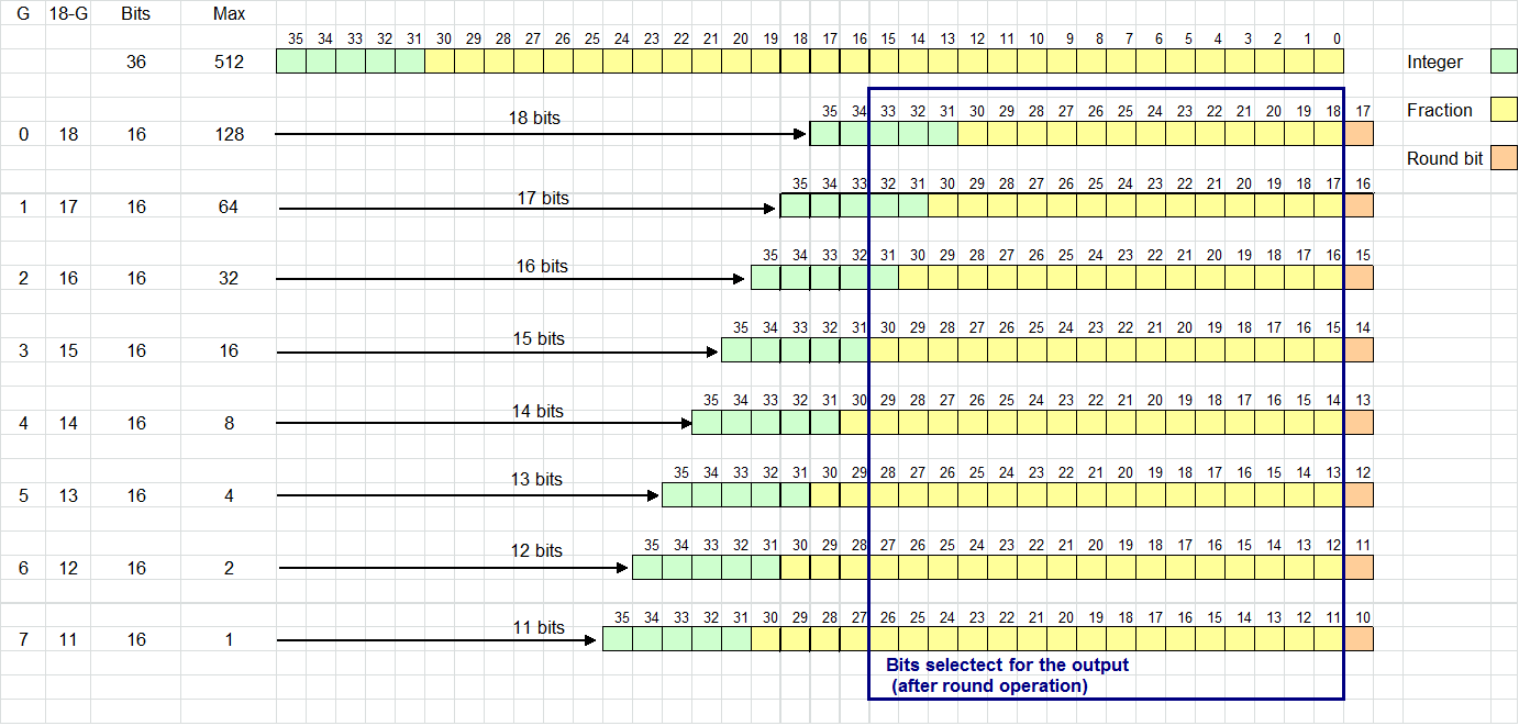 Figure 89. Shifted Output when DEC_SHIFT_SCALE=1
- Sine test mode:
- N is a 5-bit unsigned value, controlling the sine wave frequency with resolution of FS / 26, which is 0.625 MHz for 40-MHz ADC clock.
- k is 4-bit unsigned value, controlling the wave amplitude, from unity to the full scale of 14 bits, including saturation.
- C is 7-bit signed value for DC offset control.
- Coefficient output test mode:
- The input to the decimating filter can be replaced with a sequence of one impulse and zero samples, where one impulse (0x4000) is followed by (16 × M) zeros (that is, 0 × 0000).
- This mode is useful to check decimation filter coefficients.
- This mode can be enabled using register TM_COEFF_EN.
Table 17. Test Modes
| Register Name | SPI Address |
|---|---|
| TM_SINE_DC | 0x1E[15:9] |
| TM_SINE_AMP | 0x1E[8:5] |
| TM_SINE_STEP | 0x1E[4:0] |
| TM_SINE_EN | 0x1D[2] |
| TM_COEFF_EN | 0x1D[3] |
The normal ADC output can be replaced by:

The controlling values fit into one 16-bit register. This test pattern shall allow testing of demodulation, decimation filter, DC removal, gain control, and so on.
8.6.2.1 Profile RAM and Coefficient RAM
Writing data to profile RAM and coefficient RAM is similar to registers. Both RAMs do not get reset after resetting the device. RAM does not have default values, so it is necessary to write required values to RAM. RAM address values must be given to the pointer register that points to the location wherever data needs to be written. Because both RAMs are part of the demodulator, SPI_DIG_EN should be low /'0' while writing.
NOTE
TI recommends to program the profile and filter RAMs before configuring other registers.
A trigger is required to make new settings effective, such as profile RAM, coefficient RAM, and PROFILE_INDX Reg.0x0E[15:11] —either an external trigger event through the TX_SYNC_IN pin or a manual trigger event through Register 0[2].
PROFILE_INDX Reg.0x0E[15:11] must be reprogrammed to ensure new profile and filter RAMs loaded correctly.
ADC CLK is required during profile and coefficent RAM programming.
Table 18. Profile Related Registers
| Register Name | SPI Address |
|---|---|
| PROFILE_MEM_ADDR_WR | 0x08[4:0] |
| PROFILE_BANK | 0x09[63:0] |
| PROFILE_INDEX | 0x0E[15:11] |
spacer
- Profile RAM can store up to 32 vectors/profiles. Each vector/profile has 64 bits.
- Pointer value should be given to the register PROFILE_MEM_ADDR_WR before writing to RAM.
- The 64 bits of each vector/profile are arranged as follows:
Table 19. Profile RAM(2)(3)
| NAME OF PARAMETER | ADDRESS | DESCRIPTION |
|---|---|---|
| Reserved | RAM[63:50] | Set to 0 |
| Reserved | RAM[49:36] | Set to 0 |
| Pointer to coeff memory (P)(1) | RAM[35:28] | A pointer to filter coefficient memory (8 bits), pointing to 8 coefficient blocks. The relevant coefficients start from address P × 8 in the coefficients memory and will continue for M blocks. |
| Decimation Factor (M)(1) | RAM[27:22] | Decimation factor for decimation block |
| Down conversion frequency (ƒ)(1) | RAM[21:6] | Down conversion frequency for down conversion block |
| Reserved | RAM[5] | Set to 0 |
| Gain compensation factor (G)(1) | RAM[4:2] | Gain compensation factor parameter for decimation block |
8.6.2.1.1 Programming the Profile RAM
- Set SEN and SPI_DIG_EN as 0.
- Set SPI address 0xC8[4:0] with the base address, for example 0x0000. 0xC8 means both demodulator subchips are enabled.
- The 64 profile vector bits are arranged as following:
- RAM[63:50] = 0 (reserved)
- RAM[49:36] = 0 (reserved)
- RAM[35:28] = Pointer to coeff memory (8 bit)
- RAM[27:22] = Decimation factor (6 bit)
- RAM[21:6] = Demodulation frequency (16 bit)
- RAM[5] = 0
- RAM[4:2] = Gain compensation factor (3 bit)
- RAM[1:0] = 2 LSBs are ignored, can be set as zeros.
- Write the above 64 bits to SPI address 0xC9 (MSB first).
- Repeat steps 3 and 4 for the following profile entries (the address in register 0xC8 auto increments).
- Set SEN and SPI_DIG_EN as 1.
8.6.2.1.2 Procedure for Configuring Next Profile Vector
- Write profile index (5 bits) to SPI address 0xCE[15:11]. 0xCE means both demodulator subchips are enabled.
Table 20. Coefficient RAM
| Register Name | SPI Address |
|---|---|
| COEFF_MEM_ADDR_WR | 0x06[7:0] |
| COEFF_BANK | 0x07[111:0] |
| MANUAL_COEFF_START_ADDR | 0x1F[14:7] |
| MANUAL_COEFF_START_EN | 0x1F[15] |
spacer
- Coefficient RAM can store up to 256 coefficient memory blocks. The size of each block is 112 bits.
- Pointer value should be given to the register COEFF_MEM_ADDR_WR before writing to RAM.
- Write 112 bits to SPI address 0xC7 (MSB first). Each coefficient memory block consists of eight 14-bit coefficients which are aligned in the following manner: coefficient order from right to left and bit order from right to left).
Table 21. Coefficient RAM Mapping
| Coeff 7[13:0] | Coeff 6[13:0] | Coeff 5[13:0] | Coeff 4[13:0] | Coeff 3[13:0] | Coeff 2[13:0] | Coeff 1[13:0] | Coeff 0[13:0] |
|---|---|---|---|---|---|---|---|
| 111:98 | 97:84 | 83:70 | 69:56 | 55:42 | 41:28 | 27:14 | 13:0 |
NOTE
The coefficients are in 2's complement format. SPI serialization is done from left to right (0xCoeff 7[13] first and 0xCoeff 0[0] last)
spacer
- Because the decimation block uses 16 × M tap FIR filter and filter coefficients are symmetric, only half (that is 8 × M) filter coefficients are necessary to be stored (M is the decimation factor). Each 8 coefficient block that is written to the memory represents a single phase of a polyphase filter. Therefore, the relation between the filter coefficients Cn and their index (i,j) in the coefficients memory is given by:
Example for M = 4
Table 22. Coefficient RAM Mapping
| j\I | 7 | 6 | 5 | 4 | 3 | 2 | 1 | 0 |
|---|---|---|---|---|---|---|---|---|
| 0 | Coeff 31 | Coeff 27 | Coeff 23 | Coeff 19 | Coeff 15 | Coeff 11 | Coeff 7 | Coeff 3 |
| 1 | Coeff 30 | Coeff 26 | Coeff 22 | Coeff 18 | Coeff 14 | Coeff 10 | Coeff 6 | Coeff 2 |
| 2 | Coeff 29 | Coeff 25 | Coeff 21 | Coeff 17 | Coeff 13 | Coeff 9 | Coeff 5 | Coeff 1 |
| 3 | Coeff 28 | Coeff 24 | Coeff 20 | Coeff 16 | Coeff 12 | Coeff 8 | Coeff 4 | Coeff 0 |
spacer
- Coefficient start address can be given using the Pointer to Coeff Memory (P) parameter of profile RAM. Alternatively, the start address can be given using register MANUAL_COEFF_START_ADDR. (While using this register, register enable bit MANUAL_COEFF_START_EN should be set to 1.)
8.6.2.1.3 Programming the Coefficient RAM
- Set SPI address 0xC6[7:0] with the base address, for example 0x0000. 0xC6 means both demodulator subchips are enabled.
- Write 112 bits to SPI address 0xC7 (MSB first). Each coefficient memory word consists of eight 14-bit coefficients, which are aligned in the following manner: coefficient order from right to left and bit order from right to left.
- Repeat the previous step for the following coefficient bulk entries (the address in register 0xC6 auto increments).
NOTE
The coefficients are in 2s complement format.
| Coeff 7[13:0] | Coeff 6[13:0] | Coeff 5[13:0] | Coeff 4[13:0] | Coeff 3[13:0] | Coeff 2[13:0] | Coeff 1[13:0] | Coeff 0[13:0] |
| 111:98 | 97:84 | 83:70 | 69:56 | 55:42 | 41:28 | 27:14 | 13:0 |
NOTE
SPI serialization is done from left to right (Coeff 7[13] first and Coeff 0[0] last).
8.6.2.1.4 Filter Coefficent Test Mode
Coefficient test mode allows for the streaming of coefficients through the demodulator to the LVDS. Filter coefficient test mode can be set by the following:
- Enable TM_COEFF_EN.
- Write OUTPUT_RESOLUTION (0x03[11:9]) = 0b100, that is, 16-bit output. (output bit resolution of 14 bits will not give proper result.)
- Write DC_REMOVAL_BYPASS (0x0A[0]) = 1, DWN_CNV_BYPASS (0x0A[2]) = 1.
- Write DC_DEC_SHIFT_FORCE_EN (0x1D[7]) = 1, DEC_SHIFT_FORCE (0x1D[6:4] = 0b110, and DEC_SHIFT_SCALE (0x0a[13]) = 1.
- Write MODULATE_BYPASS (0x0A[14]) = 1. After writing all of the above settings, coefficients come at the output in the sequence as follow.
- M = 2
- Address 0: C15 C13 C11 C09 C07 C05 C03 C01; Address 1: C14 C12 C10 C08 C06 C04 C02 C00
- The order in which coefficients come at the output will be: 0 C01 C03 C05 C07 C09 C11 C13 C15 C14 C12 C10 C08 C06 C04 C02 C00 C00 C02 C04 C06 C08 C10 C12 C14 C15 C13 C11 C09 C07 C05 C03 C01 0
- M = 8
- The coefficients come to the output as shown in Figure 91.
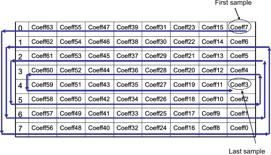
NOTE:
When it reaches the last sample, it starts giving coefficients in the reverse direction until it reaches the point it started.8.6.2.1.5 TX_SYNC and SYNC_WORD Timing
As shown in Figure 92, hardware TX_SYNC is latched at the next negative edge of the ADC Clock after 0 to 1 transition of TX_SYNC. The time gap between latched edge and the start of the LVDS SYNC_WORD is kT ns where T is the time period of ADC clock and k = 16 + decFactor + 1. tSETUP and tHOLD can be considered as 1.5 ns in the normal condition. Both are at the negative edge of the ADC clock.
8.6.2.1.6 FIR Filter Delay versus TX_TRIG Timing
The AFE5809 device’s decimation filter is a symmetric M×16-order FIR filter, where M is the decimation factor from 1 to 32. Half of the M×16 coefficients are stored in the filter coefficient memory.
For a discrete-time FIR filter, its output is a weighted sum of the current and a finite number of previous values of the input as Equation 7 shows.

where
- X[n] is the input signal.
- Y[n] is the output signal.
- CN is the filter coefficients.
- N is the filter order.
Therefore, the delay of the AFE5809 output is related to decimation factor, M. The TX_TRIG timing also plays a role in this. In the following description, M = 1 and M = 2 are used as examples to derive a generic timing relationship among TX_TRIG, AFE input, and AFE output.
The following register settings were used when the delay relationship was measured:
Table 23. Settings for evaluating FIR Filter Delay versus TX_TRIG Timing
| Register Setting | Register Setting (HEX) | Description |
|---|---|---|
| 22[0] = 1 | 0x16[0] = 1 | Enable demodulator. 0x16 belongs to ADC register |
| Profile RAM | Profile RAM | Set different decimation factor and other settings in profile RAM. |
| Coeff RAM | Coeff RAM | Write filter coefficients in coefficient memory. |
| 29[7] = 1 | 0x1D[7] = 1 | Set DEC_SHIFT_FORCE_EN |
| 10[13] = 1 | 0xA[13] = 1 | Set DEC_SHIFT_SCALE |
| 29[6:4] = 6 | 0x1D[6:4] = 6 | Set DEC_SHIFT_FORCE |
| 10[15] = 0, 10[12] = 1, 10[4] = 1, 10[1] = 1; | 0xA[15] = 0, 0xA[12] = 1, 0xA[4] = 1, 0xA[1] = 1 | RESERVED bits |
| 10[0] = 1 | 0x0A[0] = 1 | Set DC_REMOVAL_BYPASS |
| 10[10] = 1 | 0x0A[10] = 1 | Reset down conversion phase on TX_TRIG |
| 03[14:13] = 11 | 03[14:13] = 11 | SERZ_FACTOR 16X |
| 03[11:9] = 100 | 03[11:9] = 100 | OUTPUT_RESOLUTION 16X |
| 04[4] = 1 | 04[4] = 1 | MSB_FIRST |
| 11[15:0] | 0xB[15:0] | Set custom SYNC_WORD value if needed |
| 10[2]=0 | 0x0A[2]=0 | Down conversion is enabled. |
| Profile RAM[21:6]=0 | Profile RAM[21:6]=0 | Down convert frequency set to 0, that is, multiply input signal with DC. |
| Note: Even if this frequency is set to a non-zero value, it will not change the demod latency. For experiment ease, mixing with DC is performed. ADC sampling frequency and VCA LPF settings were kept such that the AFE5809’s demod sees a single pulse. | ||
When M = 1, 8 filter coefficients written in the memory are C0, C1 to C7. An impulse signal is applied at both VCA input and TX_TRIG. Due to the impulse input, coefficients start coming at the output according to timing diagram shown in Figure 93, where 20-cycle delay is observed.
 Figure 93. Expected Latency Timing When M = 1
By adjusting the timing between AFE input and TX_TRIG, the user can obtain a timing diagram similar to Figure 93.
 Figure 94. Measured Latency Timing When M = 1
By adjusting the timing between AFE input and TX_TRIG, the user can obtain a timing diagram similar to Figure 94.
When M = 2, if the impulse is given one clock before TX_TRIG signal, then the demod output after sync word gives impulse response of the filter as shown in Figure 95.
 Figure 95. Measured Latency Timing When M = 2
Figure 96 shows a generic timing diagram. The number of zeros comes before the sync word is equal to Z. The sync word comes after S number of cycles, impulse response starts coming after L number of cycles, and input impulse is given after IP cycles with respect to TX_TRIG signal. Therefore, for different decimation factor (M), values of these numbers are listed in Table 24 and Figure 96.
Table 24. Generic Latency versus Decimation Factor M(2)(3)
| M | Number of Zeros (ZNo) | Sync Word Latency (S) | Data Latency (L) | Input Impulse (IP)(1) |
|---|---|---|---|---|
| 1 | 2 | 17 | 18 | –2 |
| 2 | 3 | 18 | 19 | –1 |
| 3 | 4 | 19 | 20 | 0 |
| 4 | 5 | 20 | 21 | 1 |
| 5 | 6 | 21 | 22 | 2 |
| 6 | 7 | 22 | 23 | 3 |
| 7 | 8 | 23 | 24 | 4 |
| 8 | 9 | 24 | 25 | 5 |
| M | M + 1 | 16 + M | 17 + M | M – 3 |
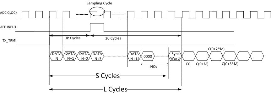 Figure 96. Measured Latency Timing at Any M
8.6.2.1.6.0.1 Expression of Decimation Filter Response
Based on Table 24, the decimation filter’s response is formulated. Figure 97 indicates that the Tx_Trig sample is considered as the reference for time scale. So, the input to the device at Tx_Trig clock will be expressed as X[0], the next sample input as X[1], and so on. Similarly, the output of the device followed by the AFE5809’s demodulator will be expressed as Y[0] at the instant of Tx_Trig, Y[1] at the next clock, and so on; Cn or C(n) indicates the coefficient of nth index.
 Figure 97. Typical Timing Expression Among ADC CLK, Input, TX_TRIG, and Output
For M = 1, the number of zeros, ZNo = 2; Sync word latency S = 17. So, the output values from sample 18 are relevant and the first few samples are:
Y[18] = C0×X[-2]+C1×X[-3]+C2×X[-4]+…+C7×X[-9]+C7×X[-10]+…+C[0]×X[-17]
Y[19] = C0×X[-1]+C1×X[-2]+C2×X[-3]+…+C7×X[-8]+C7×X[-9]+…+C[0]×X[-16]
Y[20] = C0×X[0]+C1×X[-1]+C2×X[-2]+…+C7×X[-7]+C7×X[-8]+…+C[0]×X[-15]
All these samples appear at the output because no samples are dropped for decimation factor = 1.
For M = 2, the number of zeros, ZNo = 3; Sync word latency S = 18. So, the output values from sample 19 are relevant and the first few samples are described as:
Y[19] = C0×X[-1]+C1×X[-2]+C2×X[-3]+…+C15×X[-16]+C15×X[-17]+…+C[0]×X[-32]
Y[20] = C0×X[0]+C1×X[-1]+C2×X[-2]+…+C15×X[-15]+C15×X[-16]+…+C[0]×X[-31]
Y[21] = C0×X[1]+C1×X[0]+C2×X[-1]+…+C15×X[-14]+C15×X[-15]+…+C[0]×X[-30]
But for M = 2, every alternate sample must be dropped. The decimation is adjusted in such a way that the first sample after sync is retained. Hence in this case, Y[19], Y[21], Y[23], and so forth are retained and Y[20], Y[22], Y[24], and so forth are dropped.
For M = 3, the number of zeros, ZNo = 4; Sync word latency S = 19. So, the output values from sample 20 are relevant and the first few samples are described as:
Y[20] = C0×X[0]+C1×X[-1]+C2×X[-2]+…+C23×X[-23]+C23×X[-24]+…+C[0]×X[-47]
Y[21] = C0×X[1]+C1×X[0]+C2×X[-1]+…+C23×X[-22]+C23×X[-23]+…+C[0]×X[-46]
Y[22] = C0×X[2]+C1×X[1]+C2×X[0]+…+C23×X[-21]+C23×X[-22]+…+C[0]×X[-45]
Y[23] = C0×X[3]+C1×X[2]+C2×X[1]+…+C23×X[-20]+C23×X[-21]+…+C[0]×X[-44]
But for M = 3, the last two of every three samples must be dropped. The decimation is adjusted in such a way that the first sample after sync is retained. Hence in this case, Y[20], Y[23], Y[26], and so forth are retained and Y[21], Y[22], Y[24], Y[25], and so forth are dropped.
For any M, this pattern can be generalized for a decimation factor of M. The number of ZNo = M + 1, Sync word latency S = 16 + M. So, the output values from sample (17 + M) are relevant and the first few samples are described as:
Y[17+M] = C0×X[M-3]+C1×X[M-4]+C2×X[M-5]+…+C(8M-1)×X[-7M-2]+C(8M-1)×X[-7M-3]+ … +C[0]×X[-15M-2]
Y[18+M] = C0×X[M-2]+C1×X[M-3]+C2×X[M-4]+…+C(8M-1)×X[-7M-1]+C(8M-1)×X[-7M-2]+ … +C[0]×X[-15M-1]
For a decimation factor of M which is not 1, the decimation is adjusted in such a way that the first sample after sync is retained. Hence in this case, Y[17 + M], Y[17 + 2M], Y[17 + 3M], and so forth are retained and the rest of samples between these, that is, Y[18 + M], Y[19 + 2M],…, Y[16 + 2M] are dropped.
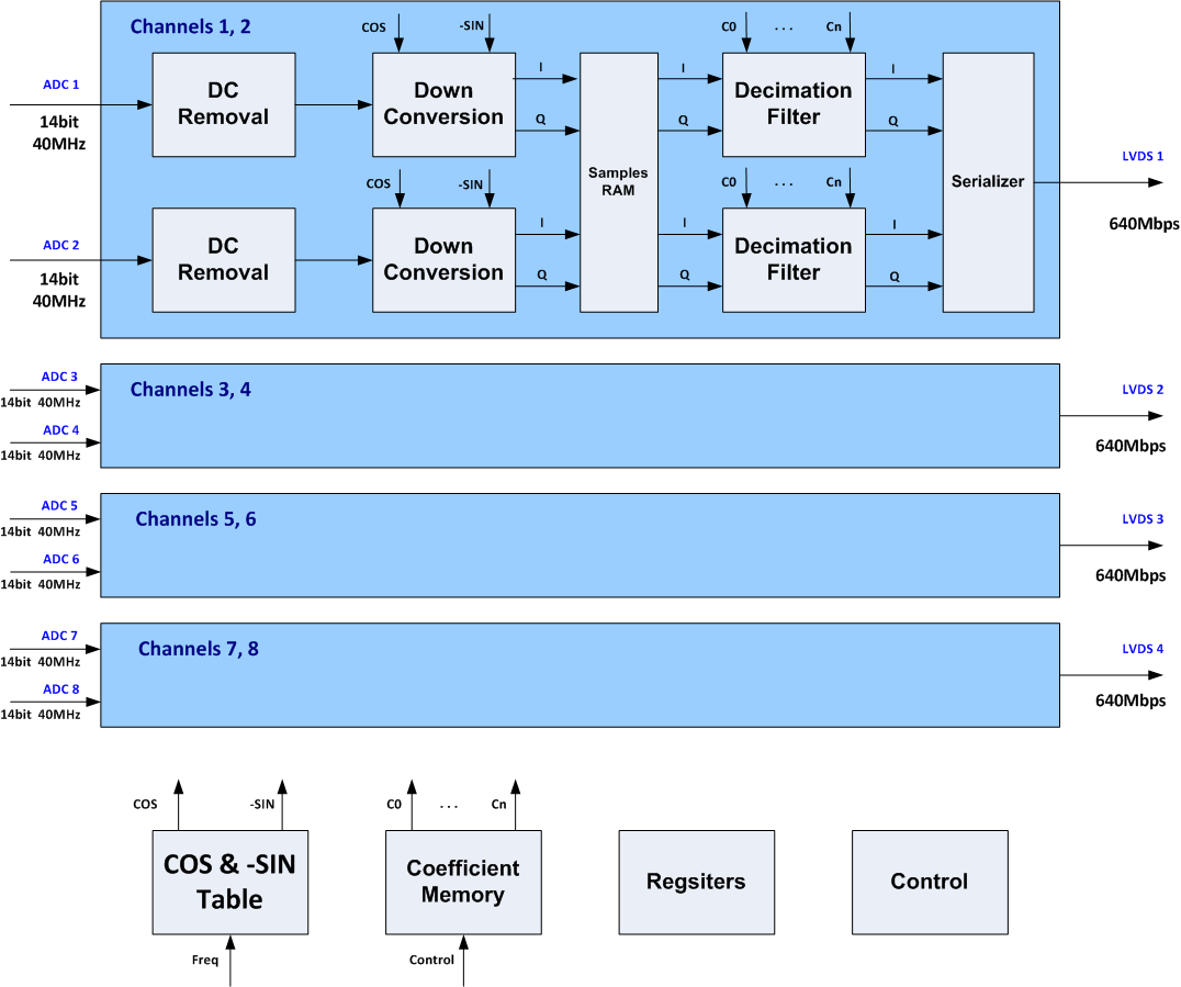
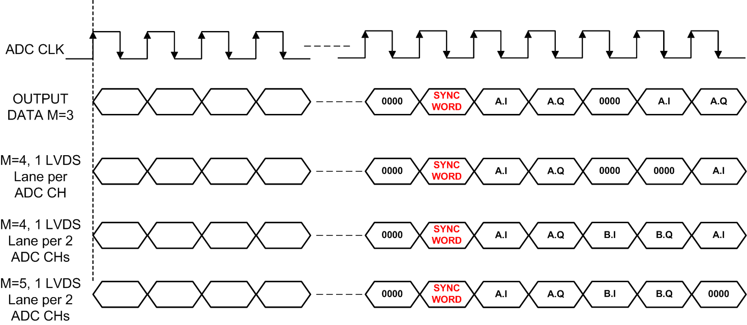
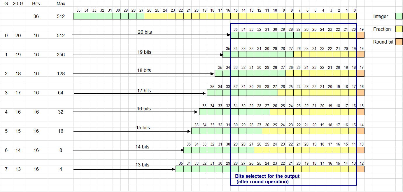
![AFE5809 Added "when DC_REMOVAL_BYPASS 10[0]
= 0" to the caption of "Sync Word Generation With Respect to TX_TRIG when
DC_REMOVAL_BYPASS 10[0] = 0 AFE5809 fig 70_slos738.png](/ods/images/SLOS738E/fig 70_slos738.png)