ZHCSM48A December 2020 – April 2021 AMC3306M05
PRODUCTION DATA
- 1 特性
- 2 应用
- 3 说明
- 4 Revision History
- 5 Pin Configuration and Functions
-
6 Specifications
- 6.1 Absolute Maximum Ratings
- 6.2 ESD Ratings
- 6.3 Recommended Operating Conditions
- 6.4 Thermal Information
- 6.5 Power Ratings
- 6.6 Insulation Specifications
- 6.7 Safety-Related Certifications
- 6.8 Safety Limiting Values
- 6.9 Electrical Characteristics
- 6.10 Switching Characteristics
- 6.11 Timing Diagrams
- 6.12 Insulation Characteristics Curves
- 6.13 Typical Characteristics
- 7 Detailed Description
- 8 Application and Implementation
- 9 Power Supply Recommendations
- 10Layout
- 11Device and Documentation Support
- 12Mechanical, Packaging, and Orderable Information
7.3.1 Analog Input
The differential amplifier input stage of the AMC3306M05 feeds a second-order, switched-capacitor, feed-forward ΔΣ modulator. The gain of the differential amplifier is set by internal precision resistors with a differential input impedance of RIND. The modulator converts the analog input signal into a bitstream that is transferred across the isolation barrier, as described in the Section 7.3.3 section.
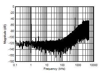
For reduced offset and offset drift, the differential amplifier is chopper-stabilized with the switching frequency set at fCLKIN / 32. As shown in Figure 7-1, the switching frequency generates a spur at 625 kHz.

| sinc3 filter, OSR = 2, fCLKIN = 20 MHz, fIN = 1 kHz |
There are two restrictions on the analog input signals INP and INN. First, if the input voltages VINP or VINN exceed the range specified in the Section 6.1 table, the input currents must be limited to the absolute maximum value, because the electrostatic discharge (ESD) protection turns on. In addition, the linearity and parametric performance of the device are ensured only when the analog input voltage remains within the linear full-scale range (VFSR) and within the common-mode input voltage range (VCM) as specified in the Section 6.3 table.