ZHCSM61C November   2014  – September 2020 CC3200MOD

PRODUCTION DATA  

  1. 特性
  2. 应用
  3. 说明
  4. Functional Block Diagrams
  5. Revision History
  6. Device Comparison
    1. 6.1 Related Products
  7. Terminal Configuration and Functions
    1. 7.1 CC3200MOD Pin Diagram
    2. 7.2 Pin Attributes
      1. 7.2.1 Module Pin Attributes
    3. 7.3 Pin Attributes and Pin Multiplexing
    4. 7.4 Recommended Pin Multiplexing Configurations
      1. 7.4.1 ADC Reference Accuracy Specifications
    5. 7.5 Drive Strength and Reset States for Analog-Digital Multiplexed Pins
    6. 7.6 Pad State After Application of Power to Chip, but Before Reset Release
  8. Specifications
    1. 8.1  Absolute Maximum Ratings
    2. 8.2  ESD Ratings
    3. 8.3  Power-On Hours (POH)
    4. 8.4  Recommended Operating Conditions
    5. 8.5  Power Consumption Summary
      1. 8.5.1 Current Consumption
    6. 8.6  Brownout and Blackout Conditions
    7. 8.7  WLAN RF Characteristics
      1. 8.7.1 WLAN Receiver Characteristics
      2. 8.7.2 WLAN Transmitter Characteristics
    8. 8.8  Reset Requirement
    9. 8.9  Thermal Resistance Characteristics for MOB and MON Packages
    10. 8.10 Timing and Switching Characteristics
      1. 8.10.1 nRESET
      2. 8.10.2 Wake Up From Hibernate Timing
  9. Detailed Description
    1. 9.1 Overview
    2. 9.2 Functional Block Diagram
    3. 9.3 Arm® Cortex®-M4 处理器内核子系统
    4. 9.4 CC3200 Device Encryption
    5. 9.5 Wi-Fi® Network Processor Subsystem
    6. 9.6 Power-Management Subsystem
      1. 9.6.1 VBAT Wide-Voltage Connection
    7. 9.7 Low-Power Operating Mode
    8. 9.8 Memory
      1. 9.8.1 External Memory Requirements
      2. 9.8.2 Internal Memory
        1. 9.8.2.1 SRAM
        2. 9.8.2.2 ROM
        3. 9.8.2.3 Memory Map
    9. 9.9 Boot Modes
      1. 9.9.1 Overview
      2. 9.9.2 Invocation Sequence and Boot Mode Selection
      3. 9.9.3 Boot Mode List
  10. 10Applications, Implementation, and Layout
    1. 10.1 Device Connection and Layout Fundamentals
      1. 10.1.1 Power Supply Decoupling and Bulk Capacitors
      2. 10.1.2 Reset
      3. 10.1.3 Unused Pins
      4. 10.1.4 General Layout Recommendations
      5. 10.1.5 Do's and Don'ts
    2. 10.2 Reference Schematics
    3. 10.3 Design Requirements
    4. 10.4 Detailed Design Procedure
    5. 10.5 Layout Recommendations
      1. 10.5.1 RF Section (Placement and Routing)
      2. 10.5.2 Antenna Placement and Routing
      3. 10.5.3 Transmission Line
  11. 11Environmental Requirements and Specifications
    1. 11.1 PCB Bending
    2. 11.2 Handling Environment
      1. 11.2.1 Terminals
      2. 11.2.2 Falling
    3. 11.3 Storage Condition
      1. 11.3.1 Moisture Barrier Bag Before Opened
      2. 11.3.2 Moisture Barrier Bag Open
    4. 11.4 Baking Conditions
    5. 11.5 Soldering and Reflow Condition
  12. 12Device and Documentation Support
    1. 12.1 Device Support
      1. 12.1.1 Development Support
      2. 12.1.2 Firmware Updates
    2. 12.2 Device Nomenclature
    3. 12.3 Documentation Support
    4. 12.4 Trademarks
  13. 13Mechanical, Packaging, and Orderable Information
    1. 13.1 Mechanical Drawing
    2. 13.2 Package Option
      1. 13.2.1 Packaging Information
      2. 13.2.2 Tape and Reel Information

请参考 PDF 数据表获取器件具体的封装图。

机械数据 (封装 | 引脚)
  • MOB|63
散热焊盘机械数据 (封装 | 引脚)

CC3200 Device Encryption

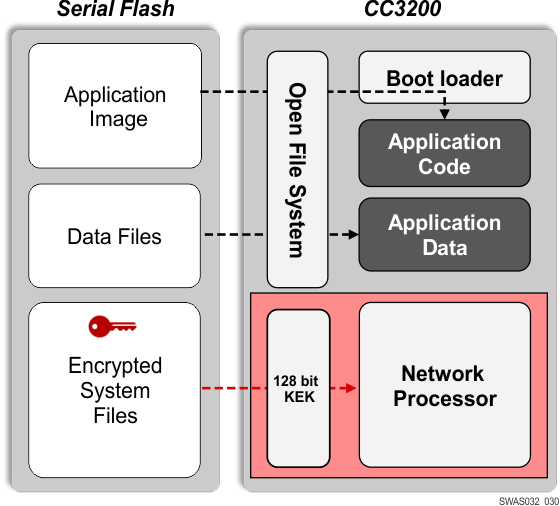
Figure 9-2 shows a standard MCU for the CC3200 device. Application image and user data files are not encrypted. Network certificates are encrypted using a device-specific key.
GUID-21272CED-5298-4939-9A85-AAF9FEFAC625-low.gifFigure 9-2 CC3200 Standard MCU