ZHCSM61C November 2014 – September 2020 CC3200MOD
PRODUCTION DATA
- 1 特性
- 2 应用
- 3 说明
- 4 Functional Block Diagrams
- 5 Revision History
- 6 Device Comparison
- 7 Terminal Configuration and Functions
-
8 Specifications
- 8.1 Absolute Maximum Ratings
- 8.2 ESD Ratings
- 8.3 Power-On Hours (POH)
- 8.4 Recommended Operating Conditions
- 8.5 Power Consumption Summary
- 8.6 Brownout and Blackout Conditions
- 8.7 WLAN RF Characteristics
- 8.8 Reset Requirement
- 8.9 Thermal Resistance Characteristics for MOB and MON Packages
- 8.10 Timing and Switching Characteristics
- 9 Detailed Description
- 10Applications, Implementation, and Layout
- 11Environmental Requirements and Specifications
- 12Device and Documentation Support
- 13Mechanical, Packaging, and Orderable Information
请参考 PDF 数据表获取器件具体的封装图。
机械数据 (封装 | 引脚)
- MOB|63
散热焊盘机械数据 (封装 | 引脚)
8.5.1 Current Consumption
TA = 25 °C, VBAT = 3.6 V
| PARAMETER | TEST CONDITIONS(1)(5) | MIN | TYP | MAX | UNIT | ||||
|---|---|---|---|---|---|---|---|---|---|
| MCU ACTIVE | NWP ACTIVE | TX | 1 DSSS | TX power level = 0 | 278 | mA | |||
| TX power level = 4 | 194 | ||||||||
| 6 OFDM | TX power level = 0 | 254 | |||||||
| TX power level = 4 | 185 | ||||||||
| 54 OFDM | TX power level = 0 | 229 | |||||||
| TX power level = 4 | 166 | ||||||||
| RX | 1 DSSS | 59 | |||||||
| 54 OFDM | 59 | ||||||||
| NWP idle connected(3) | 15.3 | ||||||||
| MCU SLEEP | NWP ACTIVE | TX | 1 DSSS | TX power level = 0 | 275 | mA | |||
| TX power level = 4 | 191 | ||||||||
| 6 OFDM | TX power level = 0 | 251 | |||||||
| TX power level = 4 | 182 | ||||||||
| 54 OFDM | TX power level = 0 | 226 | |||||||
| TX power level = 4 | 163 | ||||||||
| RX | 1 DSSS | 56 | |||||||
| 54 OFDM | 56 | ||||||||
| NWP idle connected(3) | 12.2 | ||||||||
| MCU LPDS | NWP active | TX | 1 DSSS | TX power level = 0 | 272 | mA | |||
| TX power level = 4 | 188 | ||||||||
| 6 OFDM | TX power level = 0 | 248 | |||||||
| TX power level = 4 | 179 | ||||||||
| 54 OFDM | TX power level = 0 | 223 | |||||||
| TX power level = 4 | 160 | ||||||||
| RX | 1 DSSS | 53 | |||||||
| 54 OFDM | 53 | ||||||||
| NWP LPDS(2) | 0.275 | ||||||||
| NWP idle connected(3) | 0.875 | ||||||||
| MCU hibernate | NWP hibernate | 7 | µA | ||||||
| Peak calibration current (4) | VBAT = 3.3 V | 450 | mA | ||||||
| VBAT = 2.3 V | 620 | ||||||||
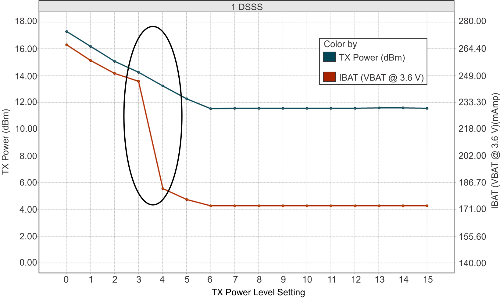
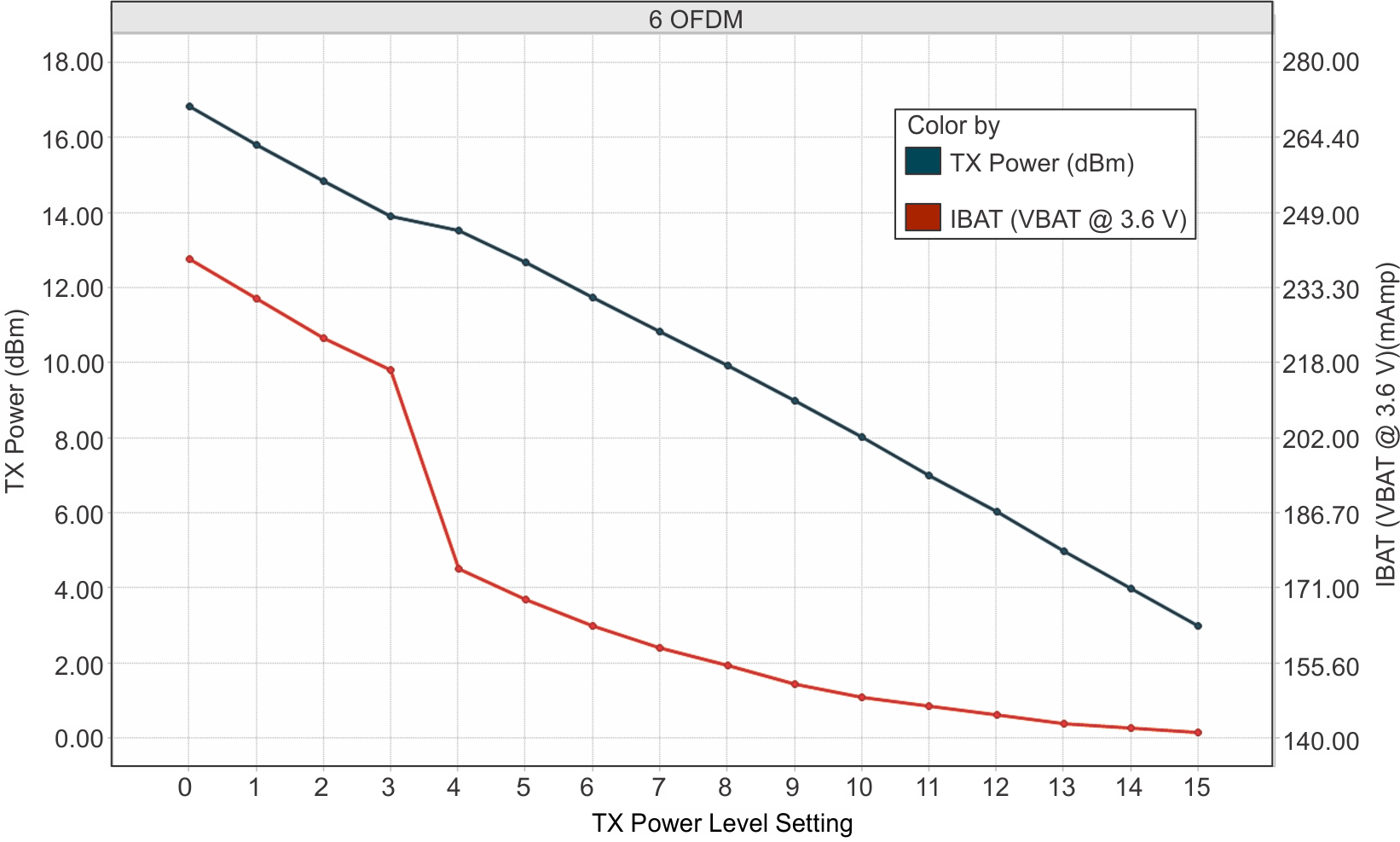
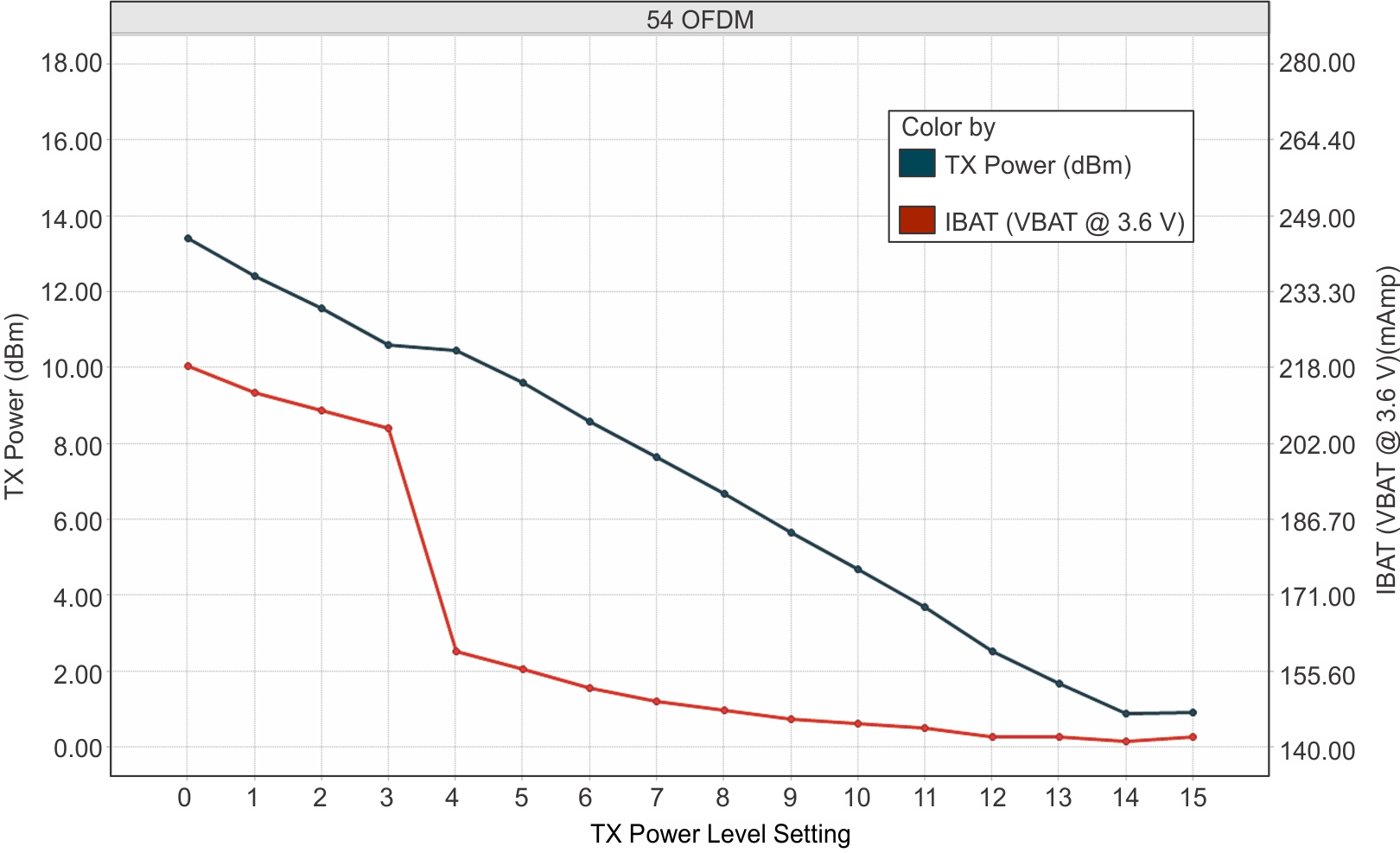
(1) TX power level = 0 implies maximum power (see Figure 8-1 through Figure 8-3). TX power level = 4 implies output power backed off approximately 4 dB.
(2) The LPDS number reported is with retention of 64KB MCU SRAM. The CC3200 device can be configured to retain 0KB, 64KB, 128KB, 192KB or 256KB SRAM in LPDS. Each 64KB retained increases LPDS current by 4 µA.
(3) DTIM = 1
(4) The complete calibration can take up to 17 mJ of energy from the battery over a time of 24 ms. Calibration is performed sparingly, typically when coming out of Hibernate and only if temperature has changed by more than 20°C or the time elapsed from prior calibration is greater than 24 hours.
(5) The CC3200 system is a constant power-source system. The active current numbers scale based on the VBAT voltage supplied.

Note: The area enclosed in the circle represents a significant reduction in current when transitioning from TX power level 3 to 4. In the case of lower range requirements (13-dBm output power), TI recommends using TX power level 4 to reduce the current.
Figure 8-1 TX Power and IBAT vs TX Power Level Settings (1 DSSS)
 Figure 8-2 TX Power and IBAT vs TX Power Level Settings (6 OFDM)
 Figure 8-3 TX Power and IBAT vs TX Power Level Settings (54 OFDM)