SCAS892C February 2010 – December 2016 CDCE937-Q1 , CDCEL937-Q1
PRODUCTION DATA.
- 1 Features
- 2 Applications
- 3 Description
- 4 Revision History
- 5 Description (continued)
- 6 Device Comparison Table
- 7 Pin Configuration and Functions
- 8 Specifications
- 9 Parameter Measurement Information
-
10Detailed Description
- 10.1 Overview
- 10.2 Functional Block Diagram
- 10.3 Feature Description
- 10.4 Device Functional Modes
- 10.5
Programming
- 10.5.1 Data Protocol
- 10.5.2 Command Code Definition
- 10.5.3 Generic Programming Sequence
- 10.5.4 Byte Write Programming Sequence
- 10.5.5 Byte Read Programming Sequence
- 10.5.6 Block Write Programming Sequence
- 10.5.7 Block Read Programming Sequence
- 10.5.8 Timing Diagram for the SDA and SCL Serial Control Interface
- 10.5.9 SDA and SCL Hardware Interface
- 10.6 Register Maps
- 11Application and Implementation
- 12Power Supply Recommendations
- 13Layout
- 14Device and Documentation Support
- 15Mechanical, Packaging, and Orderable Information
8 Specifications
8.1 Absolute Maximum Ratings
over operating free-air temperature range (unless otherwise noted)(1)| MIN | MAX | UNIT | ||
|---|---|---|---|---|
| Supply voltage, VDD | –0.5 | 2.5 | V | |
| Input voltage, VI(2)(3) | –0.5 | VDD + 0.5 | V | |
| Output voltage, VO(2) | –0.5 | Vddout + 0.5 | V | |
| Input current, II (VI < 0 and VI > VDD) | 20 | mA | ||
| Continuous output current, IO | 50 | mA | ||
| Storage temperature, Tstg | –65 | 150 | °C | |
(1) Stresses beyond those listed under Absolute Maximum Ratings may cause permanent damage to the device. These are stress ratings only, which do not imply functional operation of the device at these or any other conditions beyond those indicated under Recommended Operating Conditions. Exposure to absolute-maximum-rated conditions for extended periods may affect device reliability.
(2) The input and output negative voltage ratings may be exceeded if the input and output clamp-current ratings are observed.
(3) SDA and SCL can go up to 3.6 V as stated in the Recommended Operating Conditions.
8.2 ESD Ratings
| VALUE | UNIT | ||||
|---|---|---|---|---|---|
| V(ESD) | Electrostatic discharge | Human-body model (HBM), per AEC Q100-002(1) | ±2000 | V | |
| Charged-device model (CDM), per AEC Q100-011 |
All pins | ±500 | |||
| Corner pins | ±750 | ||||
(1) AEC Q100-002 indicates that HBM stressing shall be in accordance with the ANSI/ESDA/JEDEC JS-001 specification.
8.3 Recommended Operating Conditions
over operating free-air temperature range (unless otherwise noted)| MIN | NOM | MAX | UNIT | |||
|---|---|---|---|---|---|---|
| VDD | Device supply voltage | 1.7 | 1.8 | 1.9 | V | |
| VO | Output Yx supply voltage, Vddout | CDCE937-Q1 | 2.3 | 3.6 | V | |
| CDCEL937-Q1 | 1.7 | 1.9 | ||||
| VIL | Low-level input voltage LVCMOS | 0.3 × VDD | V | |||
| VIH | High-level input voltage LVCMOS | 0.7 × VDD | V | |||
| VI(thresh) | Input voltage threshold LVCMOS | 0.5 × VDD | V | |||
| VIS | Input voltage | S0 | 0 | 1.9 | V | |
| S1, S2, SDA, SCL; VI(thresh) = 0.5 VDD | 0 | 3.6 | ||||
| VI(CLK) | Input voltage range CLK | 0 | 1.9 | V | ||
| IOH /IOL | Output current | Vddout = 3.3 V | ±12 | mA | ||
| Vddout = 2.5 V | ±10 | |||||
| Vddout = 1.8 V | ±8 | |||||
| CL | Output load LVCMOS | 10 | pF | |||
| TA | Ambient temperature | –40 | 125 | °C | ||
| CRYSTAL/VCXO(1) | ||||||
| fXtal | Crystal input frequency (fundamental mode) | 8 | 27 | 32 | MHz | |
| ESR | Effective series resistance | 100 | Ω | |||
| fPR | Pulling range (0 V ≤ Vctrl ≤ 1.8 V)(2) | ±120 | ±150 | ppm | ||
| Vctrl | Frequency control voltage | 0 | VDD | V | ||
| C0/C1 | Pullability ratio | 220 | ||||
| CL | On-chip load capacitance at Xin and Xout | 0 | 20 | pF | ||
(1) For more information about VCXO configuration and crystal recommendation, see VCXO Application Guideline for CDCE(L)9xx Family (SCAA085).
(2) Pulling range depends on crystal-type, on-chip crystal load capacitance and PCB stray capacitance; pulling range of min ± 120 ppm applies for crystal listed in VCXO Application Guideline for CDCE(L)9xx Family (SCAA085).
8.4 Thermal Information
over operating free-air temperature range (unless otherwise noted)(1)| THERMAL METRIC(2) | CDCE937-Q1, CDCEL937-Q1 | UNIT | ||
|---|---|---|---|---|
| PW (TSSOP) | ||||
| 20 PINS | ||||
| RθJA | Junction-to-ambient thermal resistance | Airflow = 0 lfm | 89 | °C/W |
| Airflow = 150 lfm | 75 | |||
| Airflow = 200 lfm | 74 | |||
| Airflow = 250 lfm | 74 | |||
| Airflow = 500 lfm | 69 | |||
| RθJC(top) | Junction-to-case (top) thermal resistance | 31 | °C/W | |
| RθJB | Junction-to-board thermal resistance | 55 | °C/W | |
| ψJT | Junction-to-top characterization parameter | 0.8 | °C/W | |
| ψJB | Junction-to-board characterization parameter | 49 | °C/W | |
| RθJC(bot) | Junction-to-case (bottom) thermal resistance | — | °C/W | |
(1) The package thermal impedance is calculated in accordance with JESD 51 and JEDEC2S2P (high-k board).
(2) For more information about traditional and new thermal metrics, see the Semiconductor and IC Package Thermal Metrics application report.
8.5 Electrical Characteristics
over recommended operating ambient temperature range (unless otherwise noted)| PARAMETER | TEST CONDITIONS | MIN | TYP(1) | MAX | UNIT | ||
|---|---|---|---|---|---|---|---|
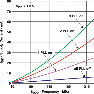
| IDD | Supply current (see Figure 1) | All outputs off, f(CLK) = 27 MHz, f(VCO) = 135 MHz |
All PLLS on | 29 | mA | ||
| Per PLL | 9 | ||||||
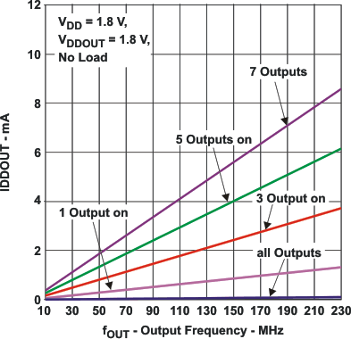
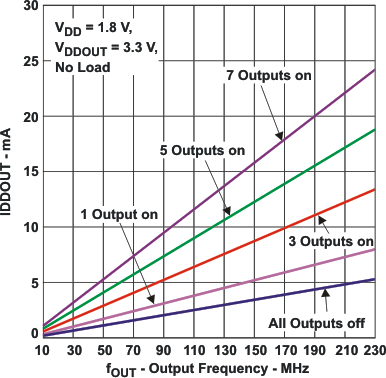
| IDDOUT | Output supply current (see Figure 2) | No load, all outputs on, fOUT = 27 MHz |
CDCE937, VDDOUT = 3.3 V |
3.1 | mA | ||
| CDCEL937, VDDOUT = 1.8 V |
1.5 | ||||||
| IDD(PD) | Power-down current | Every circuit powered down except SDA and SCL, fIN = 0 MHz, VDD = 1.9 V |
50 | µA | |||
| V(PUC) | Supply voltage Vdd threshold for power-up control circuit | 0.85 | 1.45 | V | |||
| f(VCO) | VCO frequency range of PLL | 80 | 230 | MHz | |||
| fOUT | LVCMOS output frequency | Vddout = 3.3 V | 230 | MHz | |||
| Vddout = 1.8 V | 230 | ||||||
| LVCMOS PARAMETER | |||||||
| VIK | LVCMOS input voltage | VDD = 1.7 V, II = –18 mA | –1.2 | V | |||
| II | LVCMOS input current | VI = 0 V or VDD, VDD = 1.9 V | ±5 | µA | |||
| IIH | LVCMOS input current for S0/S1/S2 | VI = VDD, VDD = 1.9 V | 5 | µA | |||
| IIL | LVCMOS input current for S0/S1/S2 | VI = 0 V, VDD = 1.9 V | –6 | µA | |||
| CI | Input capacitance at Xin/Clk | VI(Clk) = 0 V or VDD | 6 | pF | |||
| Input capacitance at Xout | VI(Xout) = 0 V or VDD | 2 | |||||
| Input capacitance at S0/S1/S2 | VIS = 0 V or VDD | 3 | |||||
| LVCMOS PARAMETER, Vddout = 3.3 V (CDCE937) | |||||||
| VOH | LVCMOS high-level output voltage | Vddout = 3 V, IOH = –0.1 mA | 2.9 | V | |||
| Vddout = 3 V, IOH = –8 mA | 2.4 | ||||||
| Vddout = 3 V, IOH = –12 mA | 2.2 | ||||||
| VOL | LVCMOS low-level output voltage | Vddout = 3 V, IOL = 0.1 mA | 0.1 | V | |||
| Vddout = 3 V, IOL = 8 mA | 0.5 | ||||||
| Vddout = 3 V, IOL = 12 mA | 0.8 | ||||||
| tPLH, tPHL | Propagation delay | All PLL bypass | 3.2 | ns | |||
| tr/tf | Rise and fall time | Vddout= 3.3 V (20%–80%) | 0.6 | ns | |||
| tjit(cc) | Cycle-to-cycle jitter(2)(3) | 1 PLL switching, Y2-to-Y3 | 60 | 90 | ps | ||
| 3 PLL switching, Y2-to-Y7 | 100 | 150 | |||||
| tjit(per) | Peak-to-peak period jitter(3) | 1 PLL switching, Y2-to-Y3 | 70 | 100 | ps | ||
| 3 PLL switching, Y2-to-Y7 | 120 | 180 | |||||
| tsk(o) | Output skew (see Table 2)(4) | fOUT = 50 MHz, Y1-to-Y3 | 60 | ps | |||
| fOUT = 50 MHz, Y2-to-Y5 | 160 | ||||||
| odc | Output duty cycle(5) | fVCO = 100 MHz, Pdiv = 1 | 45% | 55% | |||
| LVCMOS PARAMETER, Vddout = 2.5 V (CDCE937) | |||||||
| VOH | LVCMOS high-level output voltage | Vddout = 2.3 V, IOH = –0.1 mA | 2.2 | V | |||
| Vddout = 2.3 V, IOH = –6 mA | 1.7 | ||||||
| Vddout = 2.3 V, IOH = –10 mA | 1.6 | ||||||
| VOL | LVCMOS low-level output voltage | Vddout = 2.3 V, IOL = 0.1 mA | 0.1 | V | |||
| Vddout = 2.3 V, IOL = 6 mA | 0.5 | ||||||
| Vddout = 2.3 V, IOL = 10 mA | 0.7 | ||||||
| tPLH, tPHL | Propagation delay | All PLL bypass | 3.4 | ns | |||
| tr/tf | Rise and fall time | Vddout = 2.5 V (20%–80%) | 0.8 | ns | |||
| tjit(cc) | Cycle-to-cycle jitter(2) (3) | 1 PLL switching, Y2-to-Y3 | 60 | 90 | ps | ||
| 3 PLL switching, Y2-to-Y7 | 100 | 150 | |||||
| tjit(per) | Peak-to-peak period jitter(4) | 1 PLL switching, Y2-to-Y3 | 70 | 100 | ps | ||
| 3 PLL switching, Y2-to-Y7 | 120 | 180 | |||||
| tsk(o) | Output skew (see Table 2)(4) | fOUT = 50 MHz, Y1-to-Y3 | 60 | ps | |||
| fOUT = 50 MHz, Y2-to-Y5 | 160 | ||||||
| odc | Output duty cycle(5) | f(VCO) = 100 MHz, Pdiv = 1 | 45% | 55% | |||
| LVCMOS PARAMETER, Vddout = 1.8 V (CDCEL937) | |||||||
| VOH | LVCMOS high-level output voltage | Vddout = 1.7 V, IOH = –0.1 mA | 1.6 | V | |||
| Vddout = 1.7 V, IOH = –4 mA | 1.4 | ||||||
| Vddout = 1.7 V, IOH = –8 mA | 1.1 | ||||||
| VOL | LVCMOS low-level output voltage | Vddout = 1.7 V, IOL = 0.1 mA | 0.1 | V | |||
| Vddout = 1.7 V, IOL = 4 mA | 0.3 | ||||||
| Vddout = 1.7 V, IOL = 8 mA | 0.6 | ||||||
| tPLH, tPHL | Propagation delay | All PLL bypass | 2.6 | ns | |||
| tr/tf | Rise and fall time | Vddout= 1.8 V (20%–80%) | 0.7 | ns | |||
| tjit(cc) | Cycle-to-cycle jitter(2) (3) | 1 PLL switching, Y2-to-Y3 | 70 | 120 | ps | ||
| 3 PLL switching, Y2-to-Y7 | 100 | 150 | |||||
| tjit(per) | Peak-to-peak period jitter(3) | 1 PLL switching, Y2-to-Y3 | 90 | 140 | ps | ||
| 3 PLL switching, Y2-to-Y7 | 120 | 190 | |||||
| tsk(o) | Output skew (see Table 2)(4) | fOUT = 50 MHz, Y1-to-Y3 | 60 | ps | |||
| fOUT = 50 MHz, Y2-to-Y5 | 160 | ||||||
| odc | Output duty cycle(5) | f(VCO) = 100 MHz, Pdiv = 1 | 45% | 55% | |||
| SDA and SCL PARAMETER | |||||||
| VIK | SCL and SDA input clamp voltage | VDD = 1.7 V, II = –18 mA | –1.2 | V | |||
| IIH | SCL and SDA input current | VI = VDD, VDD = 1.9 V | ±10 | µA | |||
| VIH | SDA and SCL input high voltage(6) | 0.7 × VDD | V | ||||
| VIL | SDA and SCL input low voltage(6) | 0.3 × VDD | V | ||||
| VOL | SDA low-level output voltage | IOL = 3 mA, VDD = 1.7 V | 0.2 × VDD | V | |||
| CI | SCL/SDA Input capacitance | VI = 0 V or VDD | 3 | 10 | pF | ||
| EEPROM | |||||||
| EEcyc | Programming cycles of EEPROM | 1000 | cycles | ||||
| EEret | Data retention | 10 | years | ||||
(1) All typical values are at respective nominal VDD.
(2) 10000 cycles.
(3) Jitter depends on configuration. Data is taken under the following conditions: 1-PLL : fIN = 27MHz, Y2/3 = 27 MHz, (measured at Y2), 3-PLL: fIN = 27 MHz, Y2/3 = 27 MHz (measured at Y2), Y4/5 = 16.384 MHz, Y6/7 = 74.25 MHz
(4) The tsk(o) specification is only valid for equal loading of each bank of outputs, and outputs are generated from the same divider; data taking on rising edge (tr).
(5) odc depends on output rise and fall time (tr / tf).
(6) SDA and SCL pins are 3.3 V tolerant.
8.6 Timing Requirements
over recommended ranges of supply voltage, load, and operating ambient temperature (see Figure 12)| MIN | NOM | MAX | UNIT | |||
|---|---|---|---|---|---|---|
| CLK_IN | ||||||
| fCLK | LVCMOS clock input frequency | PLL bypass mode | 0 | 160 | MHz | |
| PLL mode | 8 | 160 | ||||
| tr / tf | Rise and fall time CLK signal (20% to 80%) | 3 | ns | |||
| dutyCLK | Duty cycle CLK at VDD/2 | 40% | 60% | |||
| SDA and SCL | ||||||
| fSCL | SCL clock frequency | Standard mode | 0 | 100 | kHz | |
| Fast mode | 0 | 400 | ||||
| tsu(START) | START setup time (SCL high before SDA low) | Standard mode | 4.7 | µs | ||
| Fast mode | 0.6 | |||||
| th(START) | START hold time (SCL low after SDA low) | Standard mode | 4 | µs | ||
| Fast mode | 0.6 | |||||
| tw(SCLL) | SCL low-pulse duration | Standard mode | 4.7 | µs | ||
| Fast mode | 1.3 | |||||
| tw(SCLH) | SCL high-pulse duration | Standard mode | 4 | µs | ||
| Fast mode | 0.6 | |||||
| th(SDA) | SDA hold time (SDA valid after SCL low) | Standard mode | 0 | 3.45 | µs | |
| Fast mode | 0 | 0.9 | ||||
| tsu(SDA) | SDA setup time | Standard mode | 250 | ns | ||
| Fast mode | 100 | |||||
| tr | SCL/SDA input rise time | Standard mode | 1000 | ns | ||
| Fast mode | 300 | |||||
| tf | SCL/SDA input fall time, standard mode and fast mode | 300 | ns | |||
| tsu(STOP) | STOP setup time | Standard mode | 4 | µs | ||
| Fast mode | 0.6 | |||||
| tBUS | Bus free time between a STOP and START condition | Standard mode | 4.7 | µs | ||
| Fast mode | 1.3 | |||||
8.7 Typical Characteristics
 Figure 1. CDCEx937-Q1 Supply Current
vs PLL Frequency
 Figure 3. CDCEL937-Q1 Output Current vs Output Frequency
 Figure 2. CDCE937-Q1 Output Current
vs Output Frequency