SCAS901D September 2010 – November 2017 CDCLVD1212
PRODUCTION DATA.
- 1 Features
- 2 Applications
- 3 Description
- 4 Revision History
- 5 Pin Configuration and Functions
- 6 Specifications
- 7 Parameter Measurement Information
- 8 Detailed Description
- 9 Application and Implementation
- 10Power Supply Recommendations
- 11Layout
- 12Device and Documentation Support
- 13Mechanical, Packaging, and Orderable Information
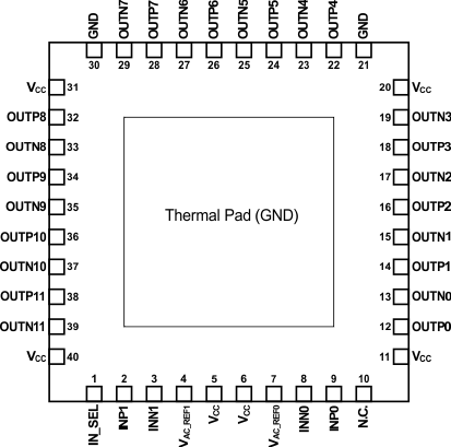
5 Pin Configuration and Functions
RHA Package
40-Pin VQFN
Top View

Pin Functions
| PIN | TYPE | DESCRIPTION | |
|---|---|---|---|
| NO. | NAME | ||
| 1 | IN_SEL | Input with an internal 200-kΩ pullup and pulldown | Input selection – selects input port (see Table 1) |
| 2, 3 | INP1, INN1 | Input | Differential redundant input pair or single-ended input |
| 4 | VAC_REF1 | Output | Bias voltage output for capacitive coupled inputs. If used, TI recommends using a 0.1-µF to GND on this pin. |
| 5, 6, 11, 20, 31, 40 | VCC | Power | 2.5-V supplies for the device |
| 7 | VAC_REF0 | Output | Bias voltage output for capacitive coupled inputs. If used, TI recommends using a 0.1-µF to GND on this pin |
| 9, 8 | INP0, INN0 | Input | Differential input pair or single-ended input |
| 10 | N.C. | — | No connect |
| 12, 13 | OUTP0, OUTN0 | Output | Differential LVDS output pair no. 0 |
| 14, 15 | OUTP1, OUTN1 | Output | Differential LVDS output pair no. 1 |
| 16, 17 | OUTP2, OUTN2 | Output | Differential LVDS output pair no. 2 |
| 18, 19 | OUTP3, OUTN3 | Output | Differential LVDS output pair no. 3 |
| 21, 30 | GND | Ground | Device ground |
| 22, 23 | OUTP4, OUTN4 | Output | Differential LVDS output pair no. 4 |
| 24, 25 | OUTP5, OUTN5 | Output | Differential LVDS output pair no. 5 |
| 26, 27 | OUTP6, OUTN6 | Output | Differential LVDS output pair no. 6 |
| 28, 29 | OUTP7, OUTN7 | Output | Differential LVDS output pair no. 7 |
| 32, 33 | OUTP8,OUTN8 | Output | Differential LVDS output pair no. 8 |
| 34, 35 | OUTP9,OUTN9 | Output | Differential LVDS output pair no. 9 |
| 36, 37 | OUTP10,OUTN10 | Output | Differential LVDS output pair no. 10 |
| 38, 39 | OUTP11,OUTN11 | Output | Differential LVDS output pair no. 11 |
| — | Thermal Pad | Ground | Device ground. Thermal pad must be soldered to ground. See thermal management recommendations |