ZHCSFP6A November 2016 – January 2017 CDCLVP111-SP
PRODUCTION DATA.
7 Detailed Description
7.1 Overview
The CDCLVP111-SP is an open emitter for LVPECL outputs. Therefore, proper biasing and termination are required to ensure correct operation of the device and to minimize signal integrity. The proper termination for LVPECL outputs is 50 Ω to (VCC – 2), but this DC voltage is not readily available on PCB. Therefore, a Thevenin equivalent circuit is worked out for the LVPECL termination in both direct-coupled (DC) and AC-coupled configurations. These configurations are shown in Figure 6 (a and b) for VCC = 2.5 V and Figure 7 (a and b) for VCC = 3.3 V, respectively. TI recommends to place all resistive components close to either the driver end or the receiver end. If the supply voltage for the driver and receiver is different, AC coupling is required.
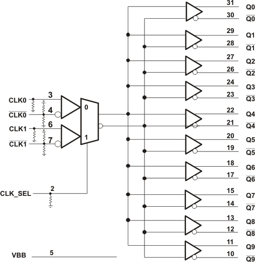
7.2 Functional Block Diagram

7.3 Feature Description
The CDCLVP111-SP is a low-additive jitter universal to LVPECL fan out buffer with 2 selectable inputs. The small package, low-output skew, and low-additive jitter make for a flexible device in demanding applications.
7.4 Device Functional Modes
Select input terminal by CLK_SEL pin.
Table 1. Function Table
| CLK_SEL | ACTIVE CLOCK INPUT |
|---|---|
| 0 | CLK0, CLK0 |
| 1 | CLK1, CLK1 |
The two inputs of the CDCLVP111-SP are internally mixed together and can be selected through the control pin. Unused inputs and outputs can be left floating to reduce overall component cost. Both AC and DC coupling schemes can be used with the CDCLVP111-SP to provide greater system flexibility.