ZHCS927G May 2012 – January 2018 CDCM6208
PRODUCTION DATA.
- 1 特性
- 2 应用
- 3 说明
- 4 修订历史记录
- 5 Pin Configuration and Functions
-
6 Specifications
- 6.1 Absolute Maximum Ratings
- 6.2 ESD Ratings
- 6.3 Recommended Operating Conditions
- 6.4 Thermal Information, Airflow = 0 LFM
- 6.5 Thermal Information, Airflow = 150 LFM
- 6.6 Thermal Information, Airflow = 250 LFM
- 6.7 Thermal Information, Airflow = 500 LFM
- 6.8 Single-Ended Input Characteristics (SI_MODE[1:0], SDI/SDA/PIN1, SCL/PIN4, SDO/ADD0/PIN2, SCS/ADD1/PIN3, STATUS1/PIN0, RESETN/PWR, PDN, SYNCN, REF_SEL)
- 6.9 Single-Ended Input Characteristics (PRI_REF, SEC_REF)
- 6.10 Differential Input Characteristics (PRI_REF, SEC_REF)
- 6.11 Crystal Input Characteristics (SEC_REF)
- 6.12 Single-Ended Output Characteristics (STATUS1, STATUS0, SDO, SDA)
- 6.13 PLL Characteristics
- 6.14 LVCMOS Output Characteristics
- 6.15 LVPECL (High-Swing CML) Output Characteristics
- 6.16 CML Output Characteristics
- 6.17 LVDS (Low-Power CML) Output Characteristics
- 6.18 HCSL Output Characteristics
- 6.19 Output Skew and Sync to Output Propagation Delay Characteristics
- 6.20 Device Individual Block Current Consumption
- 6.21 Worst Case Current Consumption
- 6.22 Timing Requirements, I2C Timing
- 6.23 Typical Characteristics
- 7 Parameter Measurement Information
-
8 Detailed Description
- 8.1 Overview
- 8.2 Functional Block Diagram
- 8.3
Feature Description
- 8.3.1 Typical Device Jitter
- 8.3.2 Universal Input Buffer (PRI_REF, SEC_REF)
- 8.3.3 VCO Calibration
- 8.3.4 Reference Divider (R)
- 8.3.5 Input Divider (M)
- 8.3.6 Feedback Divider (N)
- 8.3.7 Prescaler Dividers (PS_A, PS_B)
- 8.3.8 Phase Frequency Detector (PFD)
- 8.3.9 Charge Pump (CP)
- 8.3.10 Fractional Output Divider Jitter Performance
- 8.3.11 Device Block-Level Description
- 8.3.12 Device Configuration Control
- 8.3.13 Configuring the RESETN Pin
- 8.3.14 Preventing False Output Frequencies in SPI/I2C Mode at Start-Up
- 8.3.15 Input MUX and Smart Input MUX
- 8.4 Device Functional Modes
- 8.5 Programming
- 8.6 Register Maps
-
9 Application and Implementation
- 9.1 Application Information
- 9.2
Typical Applications
- 9.2.1 Design Requirements
- 9.2.2
Detailed Design Procedures
- 9.2.2.1 Jitter Considerations in SERDES Systems
- 9.2.2.2 Jitter Considerations in ADC and DAC Systems
- 9.2.2.3 Configuring the PLL
- 9.2.2.4 Programmable Loop Filter
- 9.2.2.5 Loop filter Component Selection
- 9.2.2.6 Device Output Signaling
- 9.2.2.7 Integer Output Divider (IO)
- 9.2.2.8 Fractional Output Divider (FOD)
- 9.2.2.9 Output Synchronization
- 9.2.2.10 Output Mux on Y4 and Y5
- 9.2.2.11 Staggered CLK Output Power Up for Power Sequencing of a DSP
- 10Power Supply Recommendations
- 11Layout
- 12器件和文档支持
- 13机械、封装和可订购信息
9.2.2.1 Jitter Considerations in SERDES Systems
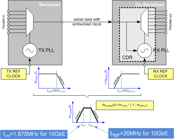
As shown in Figure 50, the bandwidth of TX and RX is the frequency range in which clock jitter adds without any attenuation to the jitter budget of the link. Outside of these frequencies, the SERDES link will attenuate clock jitter with a 20 dB/dec or even steeper roll-off.
 Figure 50. Serial Link Jitter Budget Explanation
Example: SERDES link with KeyStone™ I DSP
The SERDES TX PLL of the TI KeyStone™ I DSP family (see Hardware Design Guide for KeyStone Devices (SPRABI2)) for the SRIO interface has a 13-MHz PLL bandwidth (Low Pass Characteristic, see Figure 50). The CDCM6208V2, pin-mode 27, was characterized in this example over Process, Voltage and Temperature (PVT) with a low-pass filter of 13 MHz to simulate the TX PLL. The attenuation is higher or equal to 20 dB/dec; therefore, the characterization used 20 dB/dec as worst case.
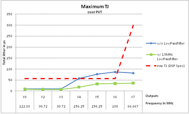
Table 41 shows the maximum total jitter over PVT with and without a low-pass filter.
Table 41. Maximum Total Jitter(1) Over PVT With and Without Low-Pass Filter
| OUTPUT | FREQUENCY
[MHz] |
MAX TJ [ps]
DSP SPEC |
MAX TJ [ps]
WITHOUT LOW-PASS FILTER |
MAX TJ [ps]
WITH 13-MHZ LOW-PASS FILTER |
|---|---|---|---|---|
| Y0 | 122.88 | 56 | 9.43 | 8.19 |
| Y2 | 30.72 | 56 | 9.60 | 7.36 |
| Y3 | 30.72 | 56 | 9.47 | 7.42 |
| Y4 | 156.25
(6 bit fraction) |
56 | 57.66 | 17.48 |
| Y5 | 156.25
(20 bit fraction) |
56 | 76.87 | 32.32 |
| Y6 | 100.00 | 56 | 86.30 | 33.86 |
| Y7 | 66.667 | 300 | 81.71 | 35.77 |
Figure 51 shows the maximum Total Jitter with and without low-pass filter characteristic and the maximum TI KeyStone™ I specification.
 Figure 51. Maximum Jitter Over PVT
NOTE
Due to the damping characteristic of the DSP SERDES PLLs, the actual TJ data can be worse.