ZHCS927G May 2012 – January 2018 CDCM6208
PRODUCTION DATA.
- 1 特性
- 2 应用
- 3 说明
- 4 修订历史记录
- 5 Pin Configuration and Functions
-
6 Specifications
- 6.1 Absolute Maximum Ratings
- 6.2 ESD Ratings
- 6.3 Recommended Operating Conditions
- 6.4 Thermal Information, Airflow = 0 LFM
- 6.5 Thermal Information, Airflow = 150 LFM
- 6.6 Thermal Information, Airflow = 250 LFM
- 6.7 Thermal Information, Airflow = 500 LFM
- 6.8 Single-Ended Input Characteristics (SI_MODE[1:0], SDI/SDA/PIN1, SCL/PIN4, SDO/ADD0/PIN2, SCS/ADD1/PIN3, STATUS1/PIN0, RESETN/PWR, PDN, SYNCN, REF_SEL)
- 6.9 Single-Ended Input Characteristics (PRI_REF, SEC_REF)
- 6.10 Differential Input Characteristics (PRI_REF, SEC_REF)
- 6.11 Crystal Input Characteristics (SEC_REF)
- 6.12 Single-Ended Output Characteristics (STATUS1, STATUS0, SDO, SDA)
- 6.13 PLL Characteristics
- 6.14 LVCMOS Output Characteristics
- 6.15 LVPECL (High-Swing CML) Output Characteristics
- 6.16 CML Output Characteristics
- 6.17 LVDS (Low-Power CML) Output Characteristics
- 6.18 HCSL Output Characteristics
- 6.19 Output Skew and Sync to Output Propagation Delay Characteristics
- 6.20 Device Individual Block Current Consumption
- 6.21 Worst Case Current Consumption
- 6.22 Timing Requirements, I2C Timing
- 6.23 Typical Characteristics
- 7 Parameter Measurement Information
-
8 Detailed Description
- 8.1 Overview
- 8.2 Functional Block Diagram
- 8.3
Feature Description
- 8.3.1 Typical Device Jitter
- 8.3.2 Universal Input Buffer (PRI_REF, SEC_REF)
- 8.3.3 VCO Calibration
- 8.3.4 Reference Divider (R)
- 8.3.5 Input Divider (M)
- 8.3.6 Feedback Divider (N)
- 8.3.7 Prescaler Dividers (PS_A, PS_B)
- 8.3.8 Phase Frequency Detector (PFD)
- 8.3.9 Charge Pump (CP)
- 8.3.10 Fractional Output Divider Jitter Performance
- 8.3.11 Device Block-Level Description
- 8.3.12 Device Configuration Control
- 8.3.13 Configuring the RESETN Pin
- 8.3.14 Preventing False Output Frequencies in SPI/I2C Mode at Start-Up
- 8.3.15 Input MUX and Smart Input MUX
- 8.4 Device Functional Modes
- 8.5 Programming
- 8.6 Register Maps
-
9 Application and Implementation
- 9.1 Application Information
- 9.2
Typical Applications
- 9.2.1 Design Requirements
- 9.2.2
Detailed Design Procedures
- 9.2.2.1 Jitter Considerations in SERDES Systems
- 9.2.2.2 Jitter Considerations in ADC and DAC Systems
- 9.2.2.3 Configuring the PLL
- 9.2.2.4 Programmable Loop Filter
- 9.2.2.5 Loop filter Component Selection
- 9.2.2.6 Device Output Signaling
- 9.2.2.7 Integer Output Divider (IO)
- 9.2.2.8 Fractional Output Divider (FOD)
- 9.2.2.9 Output Synchronization
- 9.2.2.10 Output Mux on Y4 and Y5
- 9.2.2.11 Staggered CLK Output Power Up for Power Sequencing of a DSP
- 10Power Supply Recommendations
- 11Layout
- 12器件和文档支持
- 13机械、封装和可订购信息
11.1 Layout Guidelines
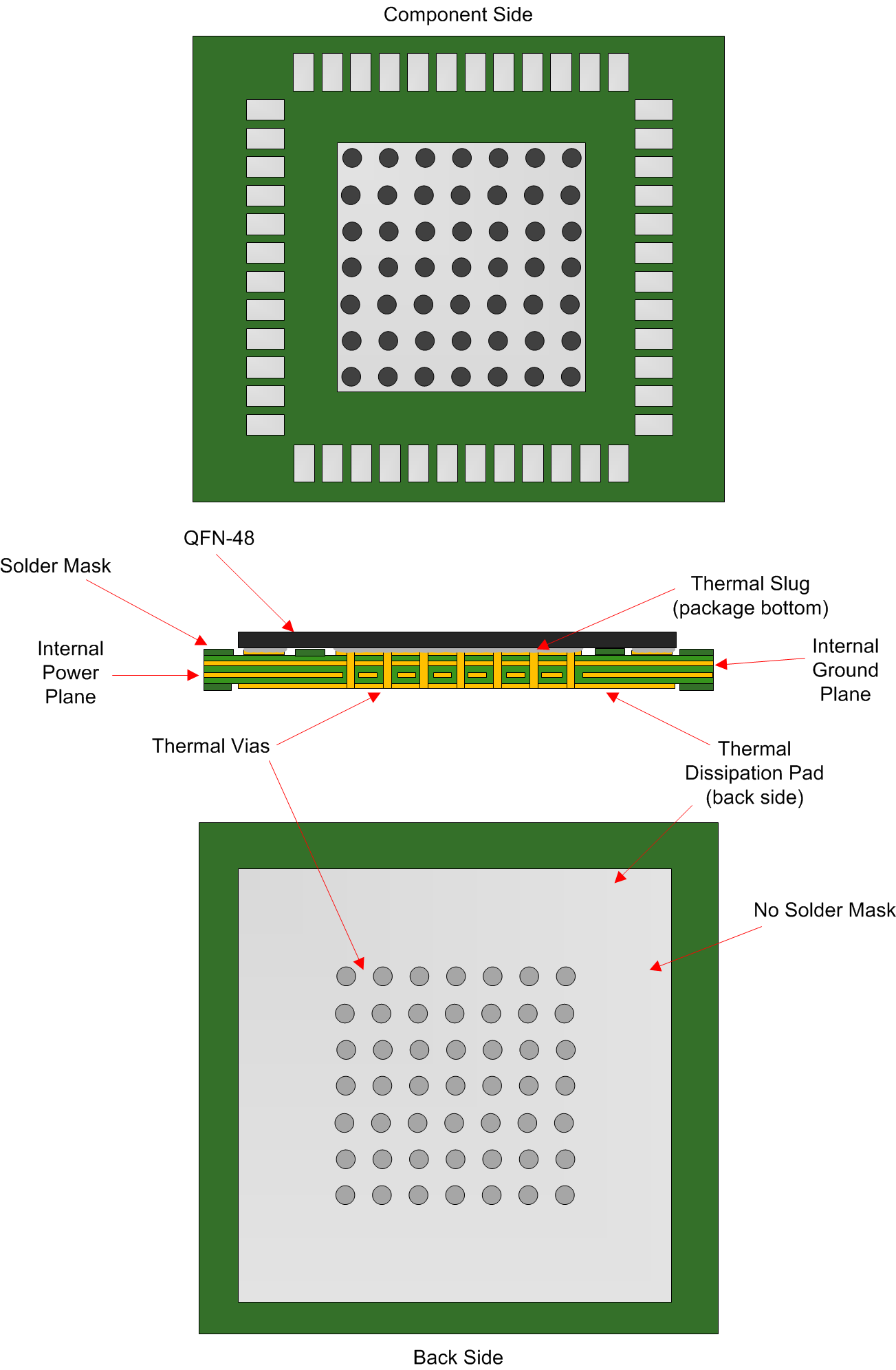
Employing the thermally enhanced printed-circuit board layout shown in Figure 64 insures good thermal performance of the solution. Observing good thermal layout practices enables the thermal pad on the backside of the VQFN-48 package to provide a good thermal path between the die contained within the package and the ambient air. This thermal pad also serves as the ground connection the device; therefore, a low inductance connection to the ground plane is essential.
Figure 64 shows a layout optimized for good thermal performance and a good power supply connection as well. The 7×7 filled via pattern facilitates both considerations.
 Figure 64. Recommended PCB Layout of CDCM6208
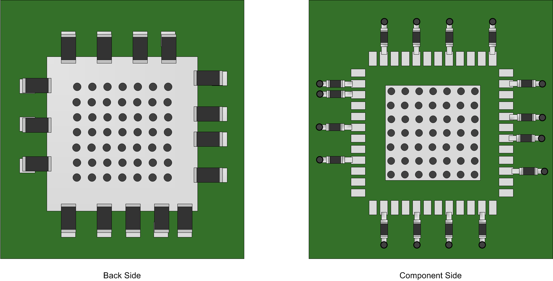
Figure 65 shows the conceptual layout detailing the recommended placement of power supply bypass capacitors. If the capacitors are mounted on the back side, 0402 components can be employed; however, soldering to the Thermal Dissipation Pad can be difficult. For component side mounting, use 0201 body size capacitors to facilitate signal routing. Keep the connections between the bypass capacitors and the power supply on the device as short as possible. Ground the other side of the capacitor using a low impedance connection to the ground plane.
 Figure 65. PCB Conceptual Layouts