SGLS390G July 2009 – November 2015 CDCM7005-SP
PRODUCTION DATA.
- 1 Features
- 2 Applications
- 3 Description
- 4 Revision History
- 5 Description (continued)
- 6 Pin Configuration and Functions
- 7 Specifications
- 8 Parameter Measurement Information
-
9 Detailed Description
- 9.1 Overview
- 9.2 Functional Block Diagram
- 9.3 Feature Description
- 9.4 Device Functional Modes
- 9.5 Programming
- 10Application and Implementation
- 11Power Supply Recommendations
- 12Layout
- 13Device and Documentation Support
- 14Mechanical, Packaging, and Orderable Information
9 Detailed Description
9.1 Overview
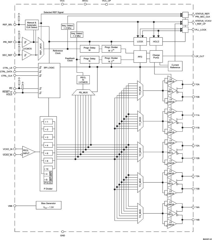
The CDCM7005-SP is a high-performance, low phase noise and low skew clock synchronizer that synchronizes a VCXO or VCO frequency to one of the two reference clocks. VC(X)O_IN clock operates up to 2.0 GHz. Through the selection of external VC(X)O and loop filter components, the PLL loop bandwidth and damping factor can be adjust to meet different system requirements.
The CDCM7005-SP can lock to one of two reference clock inputs (PRI_REF and SEC_REF), supports frequency hold-over mode and fast-frequency-locking for fail-safe and increased system redundancy. The outputs of the CDCM7005-SP are user definable and can be any combination of up to five LVPECL outputs or up to 10 LVCMOS outputs. The LVCMOS outputs are arranged in pairs (Y0A:Y0B, Y1A:Y1B, …), so that each pair has the same frequency. But each output can be separately inverted and disabled. The built in synchronization latches ensure that all outputs are synchronized for low output skew.
CDCM7005-SP is programmable through SPI (3-wire serial peripheral interface). SPI allows individually control of the device settings.
The device operates in a 3.3-V environment and is characterized for operation from –55°C to 125°C (Tcase).
9.2 Functional Block Diagram
9.3 Feature Description
9.3.1 Automatic/Manual Reference Clock Switching
The CDCM7005-SP supports two reference clock inputs, the primary clock input, PRI_REF, and the secondary clock input, SEC_REF. The clocks can be selected manually or automatically. The respective mode is selected by the dedicated SPI register bit (Word 0, Bit 30).
In the manual mode, the external REF_SEL signal selects one of the two input clocks:
REF_SEL [1] -> primary clock is selected
REF_SEL [0] -> secondary clock is selected
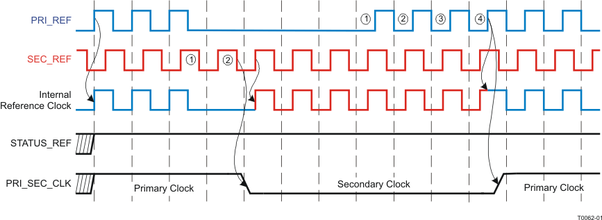
In the automatic mode, the primary clock is selected by default even if both clocks are available. In case the primary clock is not available or fails, then the input switches to the secondary clock as long until the primary clock is back. Figure 15 shows the automatic clock selection.
NOTE:
PRI_REF is the preferred clock input.In the automatic mode, the frequencies of both clock signals have to be similar, but may differ by up to 20%. The phase of the clock signal can be any.
The clock input circuitry is design to suppress glitches during switching between the primary and secondary clock in the manual and automatic mode. This avoids an undefined switching of the following circuitries.
The phase of the output clock slowly follows the new input phase. There will be no phase jump at the output. How quick the phase adjustment is done depends on the selected loop parameter, i.e., at a loop bandwidth of <100 Hz; the phase adjustment can take several ms. There is no phase build-out function supported (like in SONET/SDH applications).
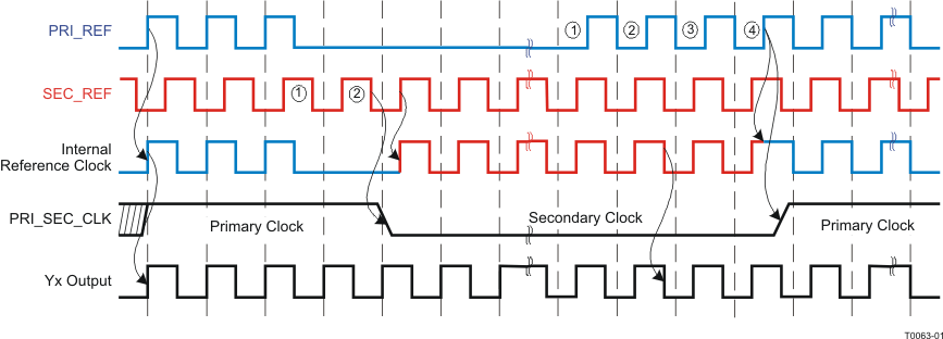 Figure 16. Phase Approach of Output to New Reference Clock
9.3.2 PLL Lock for Analog and Digital Detect
The CDCM7005-SP supports two PLL lock indications: the digital lock signal or the analog lock signal. Both signals indicate logic high-level at PLL_LOCK if the PLL locks according the selected lock condition.
9.3.2.1 PLL Lock/Out-of-Lock Definition
The PLL is locked (set high), if the rising edge of the Reference Clock (PRI_REF or SEC_REF clock) and Feedback Clock (VCXO_IN clock) at the PFD (phase frequency detect) are inside a predefined lock detect window, or if no cycle-slip appears, for a pre-defined number of successive clock cycles.
The PLL is out-of-lock (set low), if the rising edge of the Reference Clock (PRI_REF or SEC_REF clock) and Feedback Clock (VCXO_IN clock) at the PFD are outside the predefined lock detect window or if a cycle-slip appears.
Both, the lock detect window and the number of successive clock cycles are user definable (Word 3, Bit 2-6).
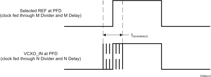 Figure 17. Lock Detect Window
The lock detect window describes the maximum allowed time difference for lock detect between the rising edge of PRI_REF or SEC_REF and VCXO_IN. The time difference is detected at the phase frequency detector. The rising edge of PRI_REF or SEC_REF is taken as reference. The rising edge of VCXO_IN is outside the lock detect window if there is a phase displacement of more than +0.5 × t(lockdetect) or –0.5 × t(lockdetect).
9.3.2.2 Digital vs Analog Lock
Figure 18 and Figure 19 show the circuit for the digital and analog lock. The analog lock operates with an external load capacitor.
When selecting the digital PLL lock option, PLL_LOCK will possibly jitter several times between lock and out of lock until a stable lock is detected. A single low-to-high step can be reached with a wide lock detect window and high number of successive clock cycles. PLL_LOCK returns to out of lock if just one cycle is outside the lock detect window or a cycle slip occurs.
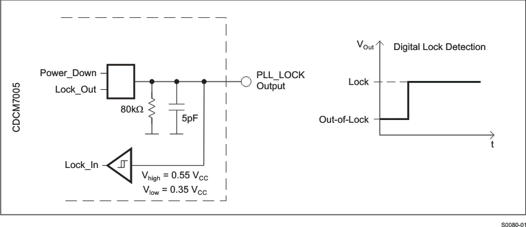 Figure 18. Digital Lock-Detect
When selecting the analog PLL Lock option, the high-pulses load the external capacitor via the internal 110-µA current source until logic high-level is reached. Therefore, more time is needed to detect logic high level, but jittering of PLL_LOCK will be suppressed in case of digital lock. The time PLL_LOCK needs to return to out of lock depends on the level of VOut, when the current source starts to unload the external capacitor.
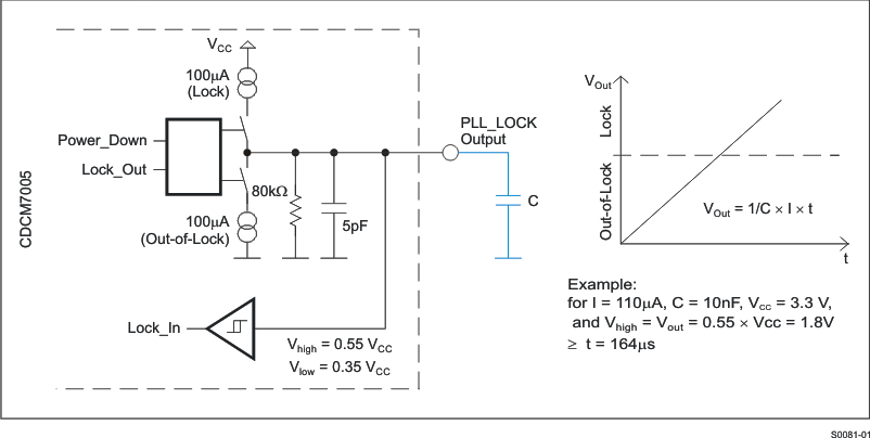 Figure 19. Analog Lock-Detect
9.3.3 Differential LVPECL Outputs and Single-Ended LVCMOS Outputs
The CDCM7005-SP supports up to 5 × LVPECL outputs or 10 × LVCMOS/LVTTL outputs or any combination of these. The single ended LVCMOS outputs are arranged in pairs which mean both outputs of a LVCMOS pair have the same frequency but can separately be disabled or inverted. The power up output arrangement is five LVPECL (default setting).
The LVPECL outputs are designed to terminate in to a 50-Ω load to VCC – 2 V. The LVCMOS outputs supports the standard LVCMOS load (see Figure 13). The LVPECL and LVCMOS outputs can be enabled (normal operation) or disabled (3-state).
In addition, the output phase can be shifted by 90 degrees when using the additional div-by-4 or div-by-8 mode of the P16-Div (see Figure 20). In the default mode (after power up), the div-by-16 mode of the P16-Div is active. To change it to a 90 degree phase shift, bit 30 or bit 31 of word 1 has to be programmed accordingly. The P 16-Div has to be selected via the dedicated YxMUX to obtain the 90 degree phase shift. The outputs are switched in pairs. When selecting the 90 degree phase shift mode, the div-by-16 functions will no longer be available. The 90 degree phase shifted signal is lagging to the non-shifted signal.
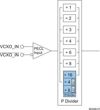 Figure 20. 90 Degree Phase Shift Option of P-Divider
Figure 21 shows the LVCMOS and LVPECL output signal when 90 degree phase shift is on.
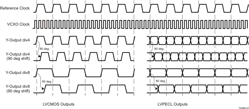 Figure 21. Output Switching Diagram
In addition, the LVCMOS supports disabled-to-low and 180° output phase shift for each output individually. When selecting the 180° phase shift together with the 90° phase shift, the respective outputs has a total phase shift of 270° (see Table 1).
Table 1. LVCMOS Phase Shift Options
| PHASE | P-DIVIDER | 180° PHASE-SHIFT | P16-Div - FUNCTION |
|---|---|---|---|
| 0° | Any P-Divider | No | div-by-16 |
| 90° | P16-Div | No | div-by-4 or div-by-8 |
| 180° | Any P-Divider | Yes | div-by-16 |
| 270° | P16-Div | Yes | div-by-4 or div-by-8 |
If the P16-Div is selected by the FB_MUX and div-by-4 or div-by-8 is active, the 90° phase shifted clock will be synchronized to PRI_REF or SEC_REF. This means all outputs Yxx, which are switched to div-by-4 or div-by-8, are in phase to PRI_REF or SEC_REF. All other outputs are 90° phase shifted with leading phase.
9.3.4 Frequency Hold-Over Mode
The HOLD function is a useful feature which helps the designer to improve the system reliability. The HOLD function holds the output frequency in case the input reference clock fails or becomes disrupted. During HOLD, the charge pump switches off (3-state) freezing the last valid output frequency. The hold function will release after a valid reference clock comes back. For proper HOLD function, the analog PLL lock detect mode has to be active.
The following register settings are involved with the HOLD function:
-
Lock Detect Window (Word 3, Bit 2, 3, 6): Defines the window in ns inside the lock is valid. The size is
3.5 ns, 8.5 ns, 18.5 ns, or a certain frequency offset. Lock sets if reference clock and the feedback clock are inside this predefined lock-detect window for a pre-selected number of successive cycles or if no frequency offset appears. - Out-of-Lock: Defines the out-of-lock condition: If the reference clock and the feedback clock at the PFD are outside the predefined Lock Detect Window or if a certain frequency offset occurs.
- Cycle-Slip (Word 3, Bit 6): A Frequency offset occurs if a certain frequency offset between reference frequency and feedback frequency (VCXO) at PFD input is detected. The minimum detectable frequency offset depends on the device setting and can be calculated:
where
- foffsetPFD = detectable frequency offset at PFD between the reference frequency (fREF) and feedback frequency (fFB)
- fPFD = frequency at phase-frequency detection circuitry
- PWD = PFD Pulse Width Delay
- Number of Clock Cycles (Word 3, Bit 4, 5): Defines the number of successive PFD cycles which have to occur inside the lock window to set Lock detect. This applies not for out-of-lock condition.
- Hold-Function (Word 3, Bit 9): Selects HOLD function (see more details below).
- Hold-Trigger (Word 3, Bit 11): Defines whether the HOLD function is always activated (Bit 11 = [1]) or whether it is dependent on the state of the analog PLL lock detect output (Bit 11 = [0]). In the latter case, HOLD is activated, if lock is set (high) and de-activated if Lock is reset (low).
- Analog PLL Lock Detect (Word 1, Bit 29): Analog lock output charges or discharges an external capacitor with every valid lock cycle. The time constant for Lock detect can be set by the value of the capacitor.
The CDCM7005 supports two types of HOLD functions, one external controllable HOLD mode and one internal mode, HOLD.
With the external HOLD function the charge pump can directly be switched into 3-state (pin H8 [BGA] or pin 14 [QFN] can be programmed for HOLD [Word 2, Bit 29]). This function is also available via SPI register (Word 2, Bit 31).
If logic low is applied to the HOLD pin, the charge pump will be switched to 3-state. After the HOLD pin is released, the charge pump is switched back in to normal operation with the next valid reference clock cycle at PRI_REF or SEC_REF and the next valid feedback clock cycle at the PFD. During HOLD, the P divider and all outputs Yx are at normal operation.
HOLD-Over-Function: The PLL has to be in lock to start the HOLD function. It switches the charge pump in to 3-State when an out-of-lock event occurs. It leaves the 3-state charge pump state when the reference clock is back. Then it starts a locking sequence of 64 cycles before it goes back to the beginning of the HOLD-over loop. The dedicated looking sequence and a digital phase alignment enable a fast lock.
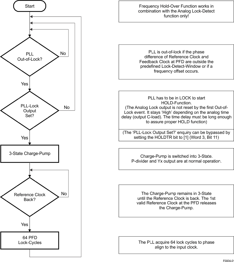 Figure 22. Frequency HOLD-Over Function
9.3.5 Charge Pump Preset to VCC_CP / 2
The preset charge pump to VCC_CP/2 is a useful feature to quickly set the center frequency of the VC(X)O after powerup or reset. The adequate control voltage for the VC(X)O will be provided to the charge-pump output by an internal voltage divider of 1 kΩ/1 kΩ to VCC_CP and GND (VCC_CP/2).
This feature helps to get the initial frequency accuracy, i.e. required at common public radio interface (CPRI) or open base station architecture initiative (OBSAI).
The preset charge pump to VCC_CP/2 can be set and reset by SPI register (word 2, bit 3). This feature must be disabled for PLL locking.
9.3.6 Charge Pump Current Direction
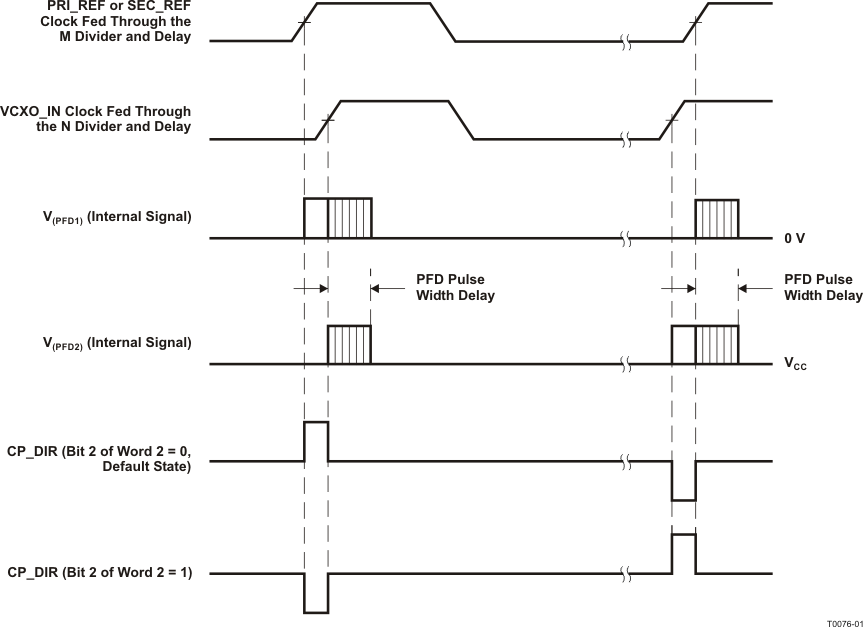
The direction of the charge pump (CP) current pulse can be changed by the SPI register (word 2, bit 2). It determines in which direction the CP current regulates (reference clock leads to feedback clock). Most applications use the positive CP output current (power-up condition) because of the use of a passive loop filter. The negative CP current is useful when using an active loop filter concept with inverting operational amplifier. Figure 23 shows the internal PFD signal and the corresponding CP current.
NOTE:
The purpose of the PFD pluse width delay is to improve spurious suppression.9.4 Device Functional Modes
Device starts up in normal operational mode and might enter RESET or power-down modes by external signal or by writing to internal SPI registers.
CDCM7005-SP enters the power-down mode if PD signal is activated (LOW) or by writing to the corresponding bit in the configuration registers R02[28]. this power-down mode resets M- and N-Divider, tri-states charge pump, STATUS_REF, or PRI_SEC_CLK pin, STATUS_VCXO or I_REF_CP pin, PLL_LOCK pin, VBB pin and all Yx outputs. This mode resets all the SPI registers to the default value. In this mode maximum current consumption is 300 µA.
CDCM7005-SP enters the RESET mode when RESET pin is activated (LOW), given that this pin is configured as RESET by R02[29], or by writing to the corresponding bit R02[30]. In case of RESET, the charge pump (CP) is switched to 3-state and all counters (N, M, P) are reset to zero (the initial divider settings are maintained in SPI registers). The LVPECL outputs are static low and high respectively and the LVCMOS outputs are all low or high if inverted. Note that RESET is not edge triggered and should have a pulse duration of at least 5 ns.
9.5 Programming
9.5.1 SPI Control Interface
The serial interface of the CDCM7005-SP is a simple SPI-compatible interface for writing to the registers of the device and consists of three control lines: CTRL_CLK, CTRL_DATA, and CTRL_LE. There are four 32 bit wide registers, which can be addressed by the two LSBs of a transferred word (bit 0 and bit 1). Every transmitted word must have 32 bits, starting with MSB first. Each word can be written separately. Bit 7, 8, 10, and Bit 12 to 31 of Word 3 are reserved for factory test purposes and must be filled with zeros. The transfer is initiated with the falling edge of CTRL_LE; as long as CTRL_LE is high, no data can be transferred. During CTRL_LE, low data can be written. The data has to be applied at CTRL_DATA and has to be stable before the rising edge of CTRL_CLK. The transmission is finished by a rising edge of CTRL_LE. With the rising edge of CTRL_LE, the new word is asynchronously transferred to the internal register (for example, N, M, P, ...). Each word has to be separately transmitted by this procedure. Unused or floating inputs must be tied to proper logic level. It is recommended to use a 20-kΩ or larger pullup resistor to VCC.
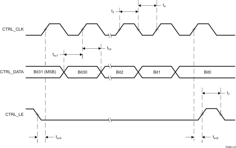 Figure 24. Timing Diagram SPI Control Interface
The SPI serial protocol accepts word Write operation only. There is neither a read, acknowledge, nor a handshake operation.
The following four words include the register settings of the programmable functions of the CDCM7005-SP. It can be modified to the customer application by changing one or more bits. It comes up with a default register setting after power up or if the power down (PD) control signal is applied. The default setting is shown in column five of the following words.
It is recommended to program Word 0, Word 1, Word 2 and Word 3 right after power up and PD becomes HIGH.
A low active function is shown as [0] and a high active function is shown as [1].
Table 2. Word 0
| BIT | BIT NAME | DESCRIPTION/FUNCTION | POWER UP CONDITION | PINS AFFECTED | |
|---|---|---|---|---|---|
| 0 | C0 | Register Selection | 0 | ||
| 1 | C1 | Register Selection | 0 | ||
| 2 | M0 | Reference Divider M | Reference Divider M Bit 0 | 1 | |
| 3 | M1 | Reference Divider M Bit 1 | 1 | ||
| 4 | M2 | Reference Divider M Bit 2 | 1 | ||
| 5 | M3 | Reference Divider M Bit 3 | 1 | ||
| 6 | M4 | Reference Divider M Bit 4 | 1 | ||
| 7 | M5 | Reference Divider M Bit 5 | 1 | ||
| 8 | M6 | Reference Divider M Bit 6 | 1 | ||
| 9 | M7 | Reference Divider M Bit 7 | 0 | ||
| 10 | M8 | Reference Divider M Bit 8 | 0 | ||
| 11 | M9 | Reference Divider M Bit 9 | 0 | ||
| 12 | N0 | VC(X)O Divider N(2) | VCXO Divider N Bit 0 | 1 | |
| 13 | N1 | VCXO Divider N Bit 1 | 1 | ||
| 14 | N2 | VCXO Divider N Bit 2 | 1 | ||
| 15 | N3 | VCXO Divider N Bit 3 | 1 | ||
| 16 | N4 | VCXO Divider N Bit 4 | 1 | ||
| 17 | N5 | VCXO Divider N Bit 5 | 1 | ||
| 18 | N6 | VCXO Divider N Bit 6 | 1 | ||
| 19 | N7 | VCXO Divider N Bit 7 | 0 | ||
| 20 | N8 | VCXO Divider N Bit 8 | 0 | ||
| 21 | N9 | VCXO Divider N Bit 9 | 0 | ||
| 22 | N10 | VCXO Divider N Bit 10 | 0 | ||
| 23 | N11 | VCXO Divider N Bit 11 | 0 | ||
| 24 | DLYM0 | Progr. Delay M | Reference Phase Delay M Bit 0 | 0 | |
| 25 | DLYM1 | Reference Phase Delay M Bit 1 | 0 | ||
| 26 | DLYM2 | Reference Phase Delay M Bit 2 | 0 | ||
| 27 | DLYN0 | Progr. Delay N | Feedback Phase Delay N Bit 0 | 0 | |
| 28 | DLYN1 | Feedback Phase Delay N Bit 1 | 0 | ||
| 29 | DLYN2 | Feedback Phase Delay N Bit 2 | 0 | ||
| 30 | MANAUT | Manual or Auto Ref. | Manual Reference Clock Selection [0] Automatic Reference Clock Selection [1] |
0 | 14, 15 |
| 31 | REFDEC | Freq. Detect | Reference Frequency Detection on [0], off [1] (1) |
0 | 50 |
detected (<2 MHz). This is useful for reference inputs frequencies less than 2 MHz where the frequency detection circuitry normally resets the STATUS_REF signal to low.
Table 3. Word 1
| BIT | BIT NAME | DESCRIPTION/FUNCTION | POWER UP CONDITION | PINS AFFECTED | |
|---|---|---|---|---|---|
| 0 | C0 | Register Selection | 1 | ||
| 1 | C1 | Register Selection | 0 | ||
| 2 | OUTSEL0 | Output (Yx) Signaling Selection | For Output Y0A, Y0B: LVPECL = enabled [1]; LVCMOS = enabled [0]; |
1 | 24, 25 |
| 3 | OUTSEL1 | For Outputs Y1A, Y1B: LVPECL = enabled [1]; LVCMOS = enabled [0]; |
1 | 29, 30 | |
| 4 | OUTSEL2 | For Outputs Y2A, Y2B: LVPECL = enabled [1]; LVCMOS = enabled [0]; |
1 | 33, 34 | |
| 5 | OUTSEL3 | For Outputs Y3A, Y3B: LVPECL = enabled [1]; LVCMOS = enabled [0]; |
1 | 37, 38 | |
| 6 | OUTSEL4 | For Outputs Y4A, Y4B: LVPECL = enabled [1]; LVCMOS = enabled [0]; |
1 | 42, 43 | |
| 7 | OUT0A0 | Output Y0 Mode | Output Y0A Mode Bit 0 | 0 | 24 |
| 8 | OUT0A1 | Output Y0A Mode Bit 1 | 0 | 24 | |
| 9 | OUT0B0 | Output Y0B Mode Bit 0 | 0 | 25 | |
| 10 | OUT0B1 | Output Y0B Mode Bit 1 | 0 | 25 | |
| 11 | OUT1A0 | Output Y1 Mode | Output Y1A Mode Bit 0 | 0 | 29 |
| 12 | OUT1A1 | Output Y1A Mode Bit 1 | 0 | 29 | |
| 13 | OUT1B0 | Output Y1B Mode Bit 0 | 0 | 30 | |
| 14 | OUT1B1 | Output Y1B Mode Bit 1 | 0 | 30 | |
| 15 | OUT2A0 | Output Y2 Mode | Output Y2A Mode Bit 0 | 0 | 33 |
| 16 | OUT2A1 | Output Y2A Mode Bit 1 | 0 | 33 | |
| 17 | OUT2B0 | Output Y2B Mode Bit 0 | 0 | 34 | |
| 18 | OUT2B1 | Output Y2B Mode Bit 1 | 0 | 34 | |
| 19 | OUT3A0 | Output Y3 Mode | Output Y3A Mode Bit 0 | 0 | 37 |
| 20 | OUT3A1 | Output Y3A Mode Bit 1 | 0 | 37 | |
| 21 | OUT3B0 | Output Y3B Mode Bit 0 | 0 | 38 | |
| 22 | OUT3B1 | Output Y3B Mode Bit 1 | 0 | 38 | |
| 23 | OUT4A0 | Output Y4 Mode | Output Y4A Mode Bit 0 | 0 | 42 |
| 24 | OUT4A1 | Output Y4A Mode Bit 1 | 0 | 42 | |
| 25 | OUT4B0 | Output Y4B Mode Bit 0 | 0 | 43 | |
| 26 | OUT4B1 | Output Y4B Mode Bit 1 | 0 | 43 | |
| 27 | SREF | Status Ref. | Displays the status of the reference clock at the STATUS_REF output [0] | 0 | 50 |
| Displays the selected clock (high for PRI_REF and low for SEC_REF clock) at the STATUS_REF output [1] |
|||||
| 28 | SXOIREF | Status VCXO or I_REF_CP | Selects STATUS_VCXO [0] | 0 | 49, 52 |
| Selects I_REF_CP [1] which enable external reference resistor used for charge pump current and analog PLL lock detect output current. | |||||
| 29 | ADLOCK | Analog or Digital Lock | Selects Digital PLL_LOCK [0] Selects Analog PLL_LOCK [1] |
0 | 52 |
| 30 | 90DIV4 | 90 degree shift div-4 | 90 degree output phase shift in div-4 mode on [1]; off [0](1) |
0 | Yx |
| 31 | 90DIV8 | 90 degree shift div-8 | 90 degree output phase shift in div-8 mode on [1]; off [0](1) |
0 | Yx |
Table 4. Word 2
| BIT | BIT NAME |
DESCRIPTION/FUNCTION | POWER UP CONDITION | PINS AFFECTED | |
|---|---|---|---|---|---|
| 0 | C0 | Register Selection | 0 | ||
| 1 | C1 | Register Selection | 1 | ||
| 2 | CP_DIR | CP Direction | Determines in which direction CP current regulates (Reference Clock leads to Feedback Clock – see Figure 23) | 0 | 8 |
| – positive CP output current [0]; – negative CP output current [1]; |
|||||
| 3 | PRECP | Preset charge pump output voltage to VCC_CP/2, on [1], off [0] | 0 | 8 | |
| 4 | CP0 | CP Current | CP Current Setting Bit 0 | 0 | 8 |
| 5 | CP1 | CP Current Setting Bit 1 | 1 | 8 | |
| 6 | CP2 | CP Current Setting Bit 2 | 0 | 8 | |
| 7 | CP3 | CP Current Setting Bit 3 | 1 | 8 | |
| 8 | PFD0 | PFD Pulse Width | PFD Pulse Width PFD Bit 0 | 0 | 8 |
| 9 | PFD1 | PFD Pulse Width PFD Bit 1 | 0 | 8 | |
| 10 | FBMUX0 | FB_MUX | Feedback MUX Select Bit 0 | 1 | |
| 11 | FBMUX1 | Feedback MUX Select Bit 1 | 0 | ||
| 12 | FBMUX2 | Feedback MUX Select Bit 2 | 1 | ||
| 13 | Y0MUX0 | Y0_MUX | Output Y0x Select Bit 0 | 1 | 24, 25 |
| 14 | Y0MUX1 | Output Y0x Select Bit 1 | 0 | 24, 25 | |
| 15 | Y0MUX2 | Output Y0x Select Bit 2 | 1 | 24, 25 | |
| 16 | Y1MUX0 | Y1_MUX | Output Y1x Select Bit 0 | 1 | 29, 30 |
| 17 | Y1MUX1 | Output Y1x Select Bit 1 | 0 | 29,30 | |
| 18 | Y1MUX2 | Output Y1x Select Bit 2 | 1 | 29,20 | |
| 19 | Y2MUX0 | Y2_MUX | Output Y2x Select Bit 0 | 1 | 33, 34 |
| 20 | Y2MUX1 | Output Y2x Select Bit 1 | 0 | 33, 34 | |
| 21 | Y2MUX2 | Output Y2x Select Bit 2 | 1 | 33, 34 | |
| 22 | Y3MUX0 | Y3_MUX | Output Y3x Select Bit 0 | 1 | 37, 38 |
| 23 | Y3MUX1 | Output Y3x Select Bit 1 | 0 | 37, 38 | |
| 24 | Y3MUX2 | Output Y3x Select Bit 2 | 1 | 37, 38 | |
| 25 | Y4MUX0 | Y4_MUX | Output Y4x Select Bit 0 | 1 | 42, 43 |
| 26 | Y4MUX1 | Output Y4x Select Bit 1 | 0 | 42, 43 | |
| 27 | Y4MUX2 | Output Y4x Select Bit 2 | 1 | 42, 43 | |
| 28 | PD | Power Down mode on [0], off [1] | 1 | Yx | |
| 29 | RESHOL | RESET or HOLD Pin definition: RESET [0] or HOLD [1] | 0 | 40 | |
| 30 | RESET | Resets all dividers [0] - (equal to RESET pin function) | 1 | ||
| 31 | HOLD | 3-state charge pump [0] - (equal to HOLD pin function) | 1 | 8 |
Table 5. Word 3
| BIT | BIT NAME |
DESCRIPTION/FUNCTION | POWER UP CONDITION | PINS AFFECTED | |
|---|---|---|---|---|---|
| 0 | Register selection | 1 | |||
| 1 | Register selection | 1 | |||
| 2 | LOCKW 0 | Lock Window | Lock-detect window Bit 0 | 1 | 52 |
| 3 | LOCKW 1 | Lock-detect window Bit 1 | 0 | 52 | |
| 4 | LOCKC0 | Lock Cycles | Number of coherent lock events Bit 0 | 0 | 52 |
| 5 | LOCKC1 | Number of coherent lock events Bit 1 | 1 | 52 | |
| 6 | FOFF | Frequency Offset | Frequency offset mode only for out-of-lock detection on [1] or off [0](1) | 0 | 52 |
| 7 | RES | RESERVED | 0 | RES | |
| 8 | RES | RESERVED | 0 | RES | |
| 9 | HOLDF | HOLD Function | Enables the frequency hold-over function on [1], off [0] | 0 | |
| 10 | RESERVED | 0 | RES | ||
| 11 | HOLDTR | HOLD Trigger Condition | HOLD function always activated [1];(2)
Triggered by analog PLL lock detect outputs [0] (if analog PLL Lock signal is set then HOLD is activated; if analog PLL lock signal is reset then HOLD is de-activated). |
0 | |
| 12 | RES | RESERVED | 0 | RES | |
| 13 | RES | RESERVED | 0 | RES | |
| 14 | RES | RESERVED | 0 | RES | |
| 15 | RES | RESERVED | 0 | RES | |
| 16 | GTME | General Test Mode Enable. Test Mode is only enabled if this bit is set to 1. | 0 | ||
| 17 | RES | RESERVED | 0 | RES | |
| 18 | RES | RESERVED | 0 | RES | |
| 19 | RES | RESERVED | 0 | RES | |
| 20 | RES | RESERVED | 0 | RES | |
| 21 | RES | RESERVED | 0 | RES | |
| 22 | RES | RESERVED | 0 | RES | |
| 23 | RES | RESERVED | 0 | RES | |
| 24 | RES | RESERVED | 0 | RES | |
| 25 | RES | RESERVED | 0 | RES | |
| 26 | RES | RESERVED | 0 | RES | |
| 27 | RES | RESERVED | 0 | RES | |
| 28 | PFDFC | PFD Frequency Control. Data provided to the PFD are feed through to the corresponding STATUS pins.(3) | 0 | 49 | |
| 29 | RES | RESERVED | 0 | RES | |
| 30 | RES | RESERVED | 0 | RES | |
| 31 | RES | RESERVED | 0 | RES |
9.5.2 Functional Description of the Logic
Table 6. Reference Divider M (Word 0)(1)
| M9 | M8 | M7 | M6 | M5 | M4 | M3 | M2 | M1 | M0 | Div by | Default |
|---|---|---|---|---|---|---|---|---|---|---|---|
| 0 | 0 | 0 | 0 | 0 | 0 | 0 | 0 | 0 | 0 | 1 | |
| 0 | 0 | 0 | 0 | 0 | 0 | 0 | 0 | 0 | 1 | 2 | |
| 0 | 0 | 0 | 0 | 0 | 0 | 0 | 0 | 1 | 0 | 3 | |
| 0 | 0 | 0 | 0 | 0 | 0 | 0 | 0 | 1 | 1 | 4 | |
| • • • |
|||||||||||
| 0 | 0 | 0 | 1 | 1 | 1 | 1 | 1 | 1 | 1 | 128 | Yes |
| • • • |
|||||||||||
| 1 | 1 | 1 | 1 | 1 | 1 | 1 | 1 | 0 | 1 | 1022 | |
| 1 | 1 | 1 | 1 | 1 | 1 | 1 | 1 | 1 | 0 | 1023 | |
| 1 | 1 | 1 | 1 | 1 | 1 | 1 | 1 | 1 | 1 | 1024 |
Table 7. VC(X)O Feedback Divider N (Word 0)(1) (2)
| N11 | N10 | N0 | N8 | N7 | N6 | N5 | N4 | N3 | N2 | N1 | N0 | Div by | Default |
|---|---|---|---|---|---|---|---|---|---|---|---|---|---|
| 0 | 0 | 0 | 0 | 0 | 0 | 0 | 0 | 0 | 0 | 0 | 0 | 1 | |
| 0 | 0 | 0 | 0 | 0 | 0 | 0 | 0 | 0 | 0 | 0 | 1 | 2 | |
| 0 | 0 | 0 | 0 | 0 | 0 | 0 | 0 | 0 | 0 | 1 | 0 | 3 | |
| 0 | 0 | 0 | 0 | 0 | 0 | 0 | 0 | 0 | 0 | 1 | 1 | 4 | |
| • • • |
|||||||||||||
| 0 | 0 | 0 | 0 | 0 | 1 | 1 | 1 | 1 | 1 | 1 | 1 | 128 | Yes |
| • • • |
|||||||||||||
| 1 | 1 | 1 | 1 | 1 | 1 | 1 | 1 | 1 | 1 | 0 | 1 | 4094 | |
| 1 | 1 | 1 | 1 | 1 | 1 | 1 | 1 | 1 | 1 | 1 | 0 | 4095 | |
| 1 | 1 | 1 | 1 | 1 | 1 | 1 | 1 | 1 | 1 | 1 | 1 | 4096 |
Table 8. Output Mode Selection for LVCMOS and LVPECL Outputs: Y0A, Y0B, Y1A …Y4B (Word 1)(1)
| OUTSELx | OUTxB1 | OUTxB0 | LVCMOS [YxB] | OUTxA1 | OUTxA0 | LVCMOS [YxA] | DEFAULT | |
|---|---|---|---|---|---|---|---|---|
| LVCMOS | 0 | 0 | 0 | Active | 0 | 0 | Active | |
| 0 | 0 | 1 | 3-state | 0 | 1 | 3-state | ||
| 0 | 1 | 0 | Inverting | 1 | 0 | Inverting | ||
| 0 | 1 | 1 | Low | 1 | 1 | Low | ||
| OUTSELx | OUTxB1 | OUTxB0 | OUTxA1 | OUTxA0 | LVCMOS [YxA] | DEFAULT | ||
| LVPECL | 1 | x | x | x | 0 | Active | Yx | |
| 1 | x | x | x | 1 | 3-state | |||
Table 9. Reference Delay M (PRI_REF or SEC_REF) and Feedback Delay N (VCXO) Phase Adjustment (Word 0)(1)
| DLYM2 / DLYN2 | DLYM1 / DLYN1 | DLYM0 / DLYN0 | PHASE OFFSET | DEFAULT |
|---|---|---|---|---|
| 0 | 0 | 0 | 0 ps | Yes |
| 0 | 0 | 1 | ±160 ps | |
| 0 | 1 | 0 | ±320 ps | |
| 0 | 1 | 1 | ±480 ps | |
| 1 | 0 | 0 | ±830 ps | |
| 1 | 0 | 1 | ±1130 ps | |
| 1 | 1 | 0 | ±1450 ps | |
| 1 | 1 | 1 | ±1750 ps |
Table 10. PFD Pulse Width Delay (Word 2)
| PFD1(1) | PFD0(1) | PFD PULSE WIDTH(1) (2) | DEFAULT(1) |
|---|---|---|---|
| 0 | 0 | 1.5 ns | Yes |
| 0 | 1 | 3 ns | |
| 1 | 0 | 4.5 ns | |
| 1 | 1 | 6 ns |
Table 11. Lock-Detect Window (Word 3)
| LOCKW1 | LOCKW0 | PHASE-OFFSET AT PFD INPUT(1) | DEFAULT |
|---|---|---|---|
| 0 | 0 | 3.5 ns | |
| 0 | 1 | 8.5 ns | Yes |
| 1 | 0 | 18.5 ns | |
| 1 | 1 | Frequency offset(2) |
- foffsetPDF = fPFD - 1/(1/fPFD + PWD)
- foffsetPFD = detectable frequency offset at PFD between the reference frequency (fREF) and feedback frequency (fFB)
- fPFD = frequency at phase-frequency detection circuitry
- PWD = PFD Pulse Width Delay
Table 12. Number of Successive Lock Events Inside the Lock Detect Window (Word 3)
| LOCKC1(1) | LOCKC0(1) | NO. OF SUCCESSIVE LOCK EVENTS(1) | DEFAULT(1) |
|---|---|---|---|
| 0 | 0 | 1 | |
| 0 | 1 | 16 | |
| 1 | 0 | 64 | Yes |
| 1 | 1 | 256 |
Table 13. Charge Pump Current (Word 2)
| CP3 | CP2 | CP1 | CP0 | TYPICAL CHARGE PUMP CURRENT | DEFAULT |
|---|---|---|---|---|---|
| 0 | 0 | 0 | 0 | 0 µA (3-state) | |
| 0 | 0 | 0 | 1 | 200 µA | |
| 0 | 0 | 1 | 0 | 400 µA | |
| 0 | 0 | 1 | 1 | 600 µA | |
| 0 | 1 | 0 | 0 | 800 µA | |
| 0 | 1 | 0 | 1 | 1 mA | |
| 0 | 1 | 1 | 0 | 1.2 mA | |
| 0 | 1 | 1 | 1 | 1.4 mA | |
| 1 | 0 | 0 | 0 | 1.6 mA | |
| 1 | 0 | 0 | 1 | 1.8 mA | |
| 1 | 0 | 1 | 0 | 2.0 mA | Yes |
| 1 | 0 | 1 | 1 | 2.2 mA | |
| 1 | 1 | 0 | 0 | 2.4 mA | |
| 1 | 1 | 0 | 1 | 2.6 mA | |
| 1 | 1 | 1 | 0 | 2.8 mA | |
| 1 | 1 | 1 | 1 | 3 mA |
Table 14. FB_MUX Selection (Word 2)
| FBMUX2 | FBMUX1 | FBMUX0 | SELECTED VC(X)O SIGNAL FOR THE PHASE DISCRIMINATOR | DEFAULT |
|---|---|---|---|---|
| 0 | 0 | 0 | Div by 1 | |
| 0 | 0 | 1 | Div by 2 | |
| 0 | 1 | 0 | Div by 3 | |
| 0 | 1 | 1 | Div by 4 | |
| 1 | 0 | 0 | Div by 6 | |
| 1 | 0 | 1 | Div by 8 | Yes |
| 1 | 1 | 0 | Div by 16(1) | |
| 1 | 1 | 1 | Div by 8 |
Table 15. YX_MUX – Output Divider Selection for Y0, Y1, Y2, Y3, Y4 (Word 2)
| YxMUX2 | YxMUX1 | YxMUX0 | SELECTED DIVIDED V(C)XO SIGNAL FOR THE Yx OUTPUTS | DEFAULT |
|---|---|---|---|---|
| 0 | 0 | 0 | Div by 1 | |
| 0 | 0 | 1 | Div by 2 | |
| 0 | 1 | 0 | Div by 3 | |
| 0 | 1 | 1 | Div by 4 | |
| 1 | 0 | 0 | Div by 6 | |
| 1 | 0 | 1 | Div by 8 | all Yx |
| 1 | 1 | 0 | Div by 16(1) | |
| 1 | 1 | 1 | Div by 8 |