SGLS390G July 2009 – November 2015 CDCM7005-SP
PRODUCTION DATA.
- 1 Features
- 2 Applications
- 3 Description
- 4 Revision History
- 5 Description (continued)
- 6 Pin Configuration and Functions
- 7 Specifications
- 8 Parameter Measurement Information
-
9 Detailed Description
- 9.1 Overview
- 9.2 Functional Block Diagram
- 9.3 Feature Description
- 9.4 Device Functional Modes
- 9.5 Programming
- 10Application and Implementation
- 11Power Supply Recommendations
- 12Layout
- 13Device and Documentation Support
- 14Mechanical, Packaging, and Orderable Information
7 Specifications
7.1 Absolute Maximum Ratings
over operating free-air temperature range (unless otherwise noted)(1)| MIN | MAX | UNIT | ||
|---|---|---|---|---|
| VCC, AVCC, VCC_CP |
Supply voltage (2) | –0.5 | 4.6 | V |
| VI | Input voltage (3) | –0.5 V | VCC + 0.5 V | V |
| VO | Output voltage (3) | –0.5 | VCC + 0.5 V | V |
| IOUT | Output current for LVPECL/LVCMOS outputs (0 < VO < VCC) |
±50 | mA | |
| IIN | Input current (VI < 0, VI > VCC) | ±20 | mA | |
| TJ | Maximum junction temperature | 150 | °C | |
| Tstg | Storage temperature | –65 | 150 | °C |
(1) Stresses beyond those listed under Absolute Maximum Ratings may cause permanent damage to the device. These are stress ratings only, which do not imply functional operation of the device at these or any other conditions beyond those indicated under Recommended Operating Conditions. Exposure to absolute-maximum-rated conditions for extended periods may affect device reliability.
(2) All supply voltages have to be supplied at the same time.
(3) The input and output negative voltage ratings may be exceeded if the input and output clamp-current ratings are observed.
7.2 ESD Ratings
| VALUE | UNIT | |||
|---|---|---|---|---|
| V(ESD) | Electrostatic discharge | Human body model (HBM), per ANSI/ESDA/JEDEC JS-001(1) | ±2500 | V |
| Charged-device model (CDM), per JEDEC specification JESD22-C101(2) | ±1500 | |||
(1) JEDEC document JEP155 states that 500-V HBM allows safe manufacturing with a standard ESD control process.
(2) JEDEC document JEP157 states that 250-V CDM allows safe manufacturing with a standard ESD control process.
7.3 Recommended Operating Conditions
| MIN | NOM | MAX | UNIT | ||
|---|---|---|---|---|---|
| VCC, AVCC | Supply voltage | 3 | 3.3 | 3.6 | V |
| VCC_CP | 2.3 | VCC | |||
| VIL | Low-level input voltage LVCMOS, see (2) | 0.3 VCC | V | ||
| VIH | High-level input voltage LVCMOS, see (2) | 0.7 VCC | V | ||
| IOH | High-level output current LVCMOS (includes all status pins) | –8 | mA | ||
| IOL | Low-level output current LVCMOS (includes all status pins) | 8 | mA | ||
| VI | Input voltage range LVCMOS | 0 | 3.6 | V | |
| VINPP | Input amplitude LVPECL (VVCXO_IN – V VCXO_IN )(1) | 0.5 | 1.3 | V | |
| VIC | Common-mode input voltage LVPECL | 1 | VCC–0.3 | V | |
| TC | Operating case temperature | –55 | 125 | °C | |
(1) VINPP minimum and maximum is required to maintain ac specifications; the actual device function tolerates at a minimum VINPP
of 150 mV.
of 150 mV.
(2) VIL and VIH are required to maintain ac specifications; the actual device function tolerates a smaller input level of 1V, if an ac-coupling to VCC/2 is provided.
7.4 Thermal Information
| THERMAL METRIC(1) | CDCM7005-SP(2) | UNIT | |
|---|---|---|---|
| HFG (CFP) | |||
| 52 PINS | |||
| RθJA | Junction-to-free-air thermal resistance(3) | 21.813 | °C/W |
| RθJC | Junction-to-case thermal resistance(4) | 0.849 | °C/W |
(1) For more information about traditional and new thermal metrics, see the Semiconductor and IC Package Thermal Metrics application report, SPRA953.
(2) Connected to GND with nine thermal vias (0.3 mm diameter).
(3) Board mounted, per JESD 51-5 methodology
(4) MIL-STD-883 test method 1012
7.5 Electrical Characteristics
over recommended operating free-air temperature range (unless otherwise noted)| PARAMETER | TEST CONDITIONS | MIN | TYP(1) | MAX | UNIT | |
|---|---|---|---|---|---|---|
| OVERALL | ||||||
| ICC_LVPECL | Supply current (ICC over frequency see Figure 2 through Figure 5) | ƒVCXO = 200 MHz, ƒREF_IN = 25 MHz, PFD = 195.3125 kHz, ICP = 2 mA, all outputs are LVPECL and Div-by-8 (load, see Figure 14) |
210 | 260 | mA | |
| ICC_LVCMOS | ƒVCXO = 200 MHz, ƒREF_IN = 25 MHz, PFD = 195.3125 kHz, ICP = 2 mA, All outputs are LVCMOS and Div-by-8 (load, 10 pF) |
120 | 160 | mA | ||
| ICCPD | Power-down current | ƒIN = 0 MHz, VCC = 3.6 V, AVCC = 3.6 V, VCC_CP = 3.6 V, VI = 0 V or VCC |
100 | 300 | µA | |
| IOZ | High-impedance state output current for Yx outputs | VO = 0 V or VCC – 0.8 V | ±40 | µA | ||
| VO = 0 V or VCC | ±100 | µA | ||||
| VI_REF_CP | Voltage on I_REF_CP (external current path for accurate charge pump current) | 12 kΩ to GND at pin 49 | 1.114 | 1.21 | 1.326 | V |
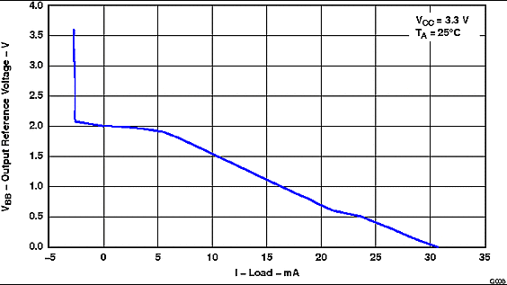
| VBB | Output reference voltage | VCC = 3 V – 3.6 V; IBB = –0.2 mA | VCC–1.446 | VCC–1.3 | VCC–1.09 | V |
| CO | Output capacitance for Yx | VCC = 3.3 V, VO = 0 V or VCC | 3 | pF | ||
| CI | Input capacitance at PRI_REF and SEC_REF | VI = 0 V or VCC, VI = 0 V or VCC | 3.6 | pF | ||
| Input capacitance at CTRL_LE, CTRL_CLOCK, CTRL_DATA | VI = 0 V or VCC | 3 | ||||
| LVCMOS | ||||||
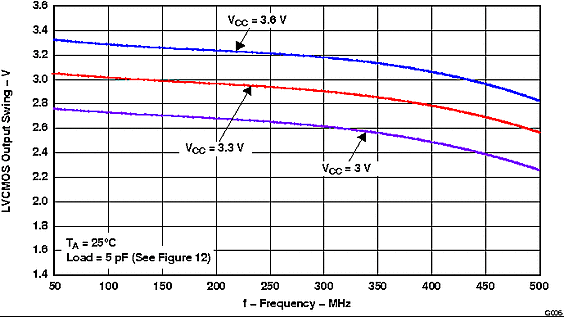
| ƒclk | Output frequency (see (2), (3), Figure 7, and Figure 8) | Load = 5 pF to GND, 1 kΩ to VCC, 1 kΩ to GND | 240 | MHz | ||
| VIK | LVCMOS input clamp voltage | VCC = 3 V, II = –18 mA | –1.2 | V | ||
| II | LVCMOS input current for CTRL_LE, CTRL_CLK, CTRL_DATA | VI = 0 V or VCC, VCC = 3.6 V | ±5 | µA | ||
| IIH | LVCMOS input current for PD, RESET, HOLD, REF_SEL, PRI_REF, SEC_REF, (see (4)) | VI = VCC, VCC = 3.6 V | 5 | µA | ||
| IIL | LVCMOS input current for PD, RESET, HOLD, REF_SEL, PRI_REF, SEC_REF (see (4)) | VI = 0 V, VCC = 3.6 V | –15 | –35 | µA | |
| VOH | High-level output voltage for LVCMOS outputs | VCC = min to max, IOH = –100 μA |
VCC–0.1 | V | ||
| VCC = 3 V, IOH = –6 mA | 2.4 | |||||
| VCC = 3 V, IOH = –12 mA | 2 | |||||
| VOL | Low-level output voltage for LVCMOS outputs | VCC = min to max, IOL = 100 μA |
0.1 | V | ||
| VCC = 3 V, IOL = 6 mA | 0.5 | |||||
| VCC = 3 V, IOL = 12 mA | 0.8 | |||||
| IOH | High-level output current | VCC = 3.3 V, VO = 1.65 V | –50 | –30 | –20 | mA |
| IOL | Low-level output current | VCC = 3.3 V, VO = 1.65 V | 20 | 30 | 50 | mA |
| tpho | Phase offset (REF_IN to Y output)(6) | VREF_IN = VCC/2, Y = VCC/2, see Figure 12, Load = 10 pF |
2.7 | ns | ||
| tsk(p) | LVCMOS pulse skew, see Figure 11 | Crosspoint to VCC/2 load, see Figure 13 | 160 | ps | ||
| tpd(LH) | Propagation delay from VCXO_IN to Yx, see Figure 11 | Crosspoint to VCC/2, Load = 10 pF, see Figure 13 (PLL bypass mode) |
2.8 | ns | ||
| tpd(HL) | ||||||
| tsk(o) | LVCMOS single-ended output skew, see (7) and Figure 11 | All outputs have the same divider ratio | 80 | ps | ||
| Outputs have different divider ratios | 80 | |||||
| Duty cycle | LVCMOS | VCC/2 to VCC/2 | 49% | 51% | ||
| tslew-rate | Output rise/fall slew rate | 20% to 80% of swing (load see Figure 13) |
3.5 | V/ns | ||
| LVPECL | ||||||
| ƒclk | Output frequency, see (3) and Figure 6 | Load, see Figure 14 | 0 | 2000 | MHz | |
| II | LVPECL input current | VI = 0 V or VCC | ±20 | µA | ||
| VOH | LVPECL high-level output voltage | Load, See Figure 14 | VCC–1.18 | VCC–0.81 | V | |
| VOL | LVPECL low-level output voltage | Load, See Figure 14 | VCC–2 | VCC–1.55 | V | |
| |VOD| | Differential output voltage | See Figure 10 and load, see Figure 14 | 500 | mV | ||
| tpho | Phase offset (REF_IN to Y output)(7) | VREF_IN = VCC/2 to cross point of Y, see Figure 12 | 250 | ps | ||
| tpd(LH) | Propagation delay time, VCXO_IN to Yx, see Figure 11 | Cross point-to-cross point, load see Figure 14 |
615 | ps | ||
| tpd(HL) | ||||||
| tsk(p) | LVPECL pulse skew, see Figure 11 | Cross point-to-cross point, load see Figure 14 |
15 | ps | ||
| tsk(o) | LVPECL output skew(7) | Load see Figure 14, all outputs have the same divider ratio | 20 | ps | ||
| Load see Figure 14, outputs have different divider ratios |
50 | |||||
| tr / tf | Rise and fall time | 20% to 80% of VOUTPP, see Figure 10 | 170 | ps | ||
| CI | Input capacitance at VCXO_IN, VCXO_IN | 2.5 | pF | |||
| LVCMOS-TO-LVPECL | ||||||
| tsk(P_C) | Output skew between LVCMOS and LVPECL outputs, see (8) and Figure 11 | Cross point to VCC/2; load, see Figure 13 and Figure 14 |
2 | 3.2 | ns | |
| PLL ANALOG LOCK | ||||||
| IOH | High-level output current | VCC = 3.6 V, VO = 1.8 V | –150 | –110 | –80 | µA |
| IOL | Low-level output current | VCC = 3.6 V, VO = 1.8 V | 80 | 110 | 150 | µA |
| IOZH LOCK | High-impedance state output current for PLL LOCK output(5) | VO = 3.6 V (PD is set low) | 45 | 65 | µA | |
| IOZL LOCK | High-impedance state output current for PLL LOCK output(5) | VO = 0 V (PD is set low) | ±5 | µA | ||
| VIT+ | Positive input threshold voltage | VCC = min to max | VCC×0.55 | V | ||
| VIT– | Negative input threshold voltage | VCC = min to max | VCC×0.35 | V | ||
| PHASE DETECTOR | ||||||
| ƒCPmax | Maximum charge pump frequency | Default PFD pulse width delay | 100 | MHz | ||
| CHARGE PUMP | ||||||
| ICP | Charge pump sink/source current range (9) | VCP = 0.5 VCC_CP | ±0.2 | ±3.9 | mA | |
| ICP3St | Charge pump 3-state current | Temperature = 25°C, 0.5 V < VCP < VCC_CP – 0.5 V | –10 | 10 | nA | |
| Temperature = –55°C to 125°C, 0.5 V < VCP < VCC_CP – 0.5 V | –50 | 50 | ||||
| ICPA | ICP absolute accuracy | VCP = 0.5 VCC_CP, internal reference resistor, SPI default settings | –20% | 10% | 20% | |
| VCP = 0.5 VCC_CP, external reference resistor 12 kΩ (1%) at I_REF_CP, SPI default settings | 5% | |||||
| ICPM | Sink/source current matching | 0.5 V < VCP < VCC_CP – 0.5 V, SPI default settings | –7% | 2.5% | 7% | |
| IVCPM | ICP vs VCP matching | 0.5 V < VCP < VCC_CP – 0.5 V | –10% | 5% | 10% | |
(1) All typical values are at VCC = 3.3 V, temperature = 25°C.
(2) ƒclk can be up to 400 MHz in the typical operating mode (25°C / 3.3-V VCC).
(3) Operating the LVCMOS or LVPECL output above the maximum frequency will not cause a malfunction to the device, but the output signal swing may no longer meet the output specification.
(4) These inputs have an internal 150-kΩ pullup resistor.
(5) Lock output has an 80-kΩ pulldown resistor.
(6) This is valid only for the same frequency of REF_IN clock and Y output clock. It can be adjusted by the SPI controller (reference delay M and VCXO delay N).
(7) The tsk(o) specification is only valid for equal loading of all outputs.
(8) The phase of LVCMOS is lagging in reference to the phase of LVPECL.
(9) Defined by SPI settings.
7.6 Timing Requirements
over recommended ranges of supply voltage, load and operating free air temperature| MIN | TYP | MAX | UNIT | ||
|---|---|---|---|---|---|
| PRI_REF/SEC_REF_IN REQUIREMENTS | |||||
| ƒREF_IN | LVCMOS primary or secondary reference clock frequency(1) (4) | 0 | 200 | MHz | |
| tr/ tf | Rise and fall time of PRI_REF or SEC_REF signals from 20% to 80% of VCC | 4 | ns | ||
| dutyREF | Duty cycle of PRI_REF or SEC_REF at VCC/2 | 40% | 60% | ||
| VCXO_IN, VCXO_IN REQUIREMENTS | |||||
| ƒVCXO_IN | VCXO clock frequency(2) | 0 | 2000 | MHz | |
| tr/ tf | Rise and fall time 20% to 80% of VINPP at 80 MHz to 800 MHz(3) | 3 | ns | ||
| dutyVCXO | Duty cycle of VCXO clock | 40% | 60% | ||
| SPI/CONTROL REQUIREMENTS (see Figure 24) | |||||
| ƒCTRL_CLK | CTRL_CLK frequency | 20 | MHz | ||
| tsu1 | CTRL_DATA to CTRL_CLK setup time | 10 | ns | ||
| th2 | CTRL_DATA to CTRL_CLK hold time | 10 | ns | ||
| t3 | CTRL_CLK high duration | 25 | ns | ||
| t4 | CTRL_CLK low duration | 25 | ns | ||
| tsu5 | CTRL_LE to CTRL_CLK setup time | 10 | ns | ||
| tsu6 | CTRL_CLK to CTRL_LE setup time | 10 | ns | ||
| t7 | CTRL_LE pulse width | 20 | ns | ||
| tr/ tf | Rise and fall time of CTRL_DATA CTRL_CLK, CTRL_LE from 20% to 80% of VCC | 4 | ns | ||
| PD, RESET, HOLD , REF_SEL REQUIREMENTS | |||||
| tr / tf | Rise and fall time of the PD, RESET, HOLD, REF_SEL signal from 20% to 80% of VCC | 4 | ns | ||
(1) At Reference Clock less than 2 MHz, the device stays in normal operation mode but the frequency detection circuitry resets the STATUS_REF signal to low. In this case, the status of the STATUS_REF is no longer relevant.
(2) If the Feedback Clock (derives from VCXO input) is less than 2 MHz, the device stays in normal operation mode but the frequency detection circuitry resets the STATUS_VCXO signal and PLL_LOCK signal to low. Both status signals are no longer relevant. This effects the HOLD-over function as well, as the PLL_LOCK signal is no longer valid!
(3) Use a square wave for lower frequencies (<80 MHz).
(4) ƒREF_IN can be up to 250 MHz in typical operating mode (25°C / 3.3-V VCC).
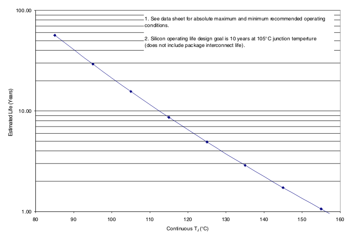 Figure 1. CDCM7005-SPHFG-V - 52-Pin HFG Package
Operating Life Derating Chart
7.7 Typical Characteristics
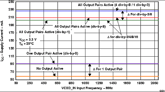
If div-by-2/4/8/16 is activated for one or more outputs, 'Δ for div-by-2/4/8/16' has to be added to ICC of div-by-1. If div-by-3 or div-by-6 is activated, 'Δ for div-by-2/4/8/16' and 'Δ for div-by-3/6' has to be added to ICC of div-by-1.
Figure 2. LVPECL Supply Current vs Number of Active Outputs
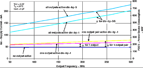
To estimate ICC with different P-divider settings use 'Δ for div-by-2/4/8/16' and 'Δ for div-by-3/6' of Figure 2
Figure 4. LVCMOS Supply Current / Device Power Consumption vs Number Of Active Outputs (Load = 5 pF)
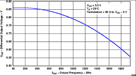
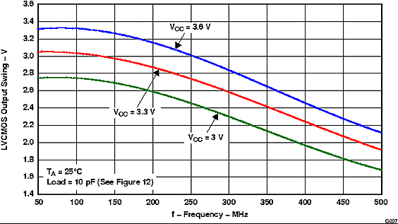
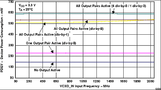
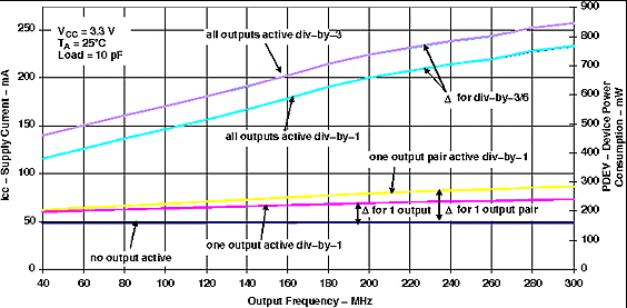
To estimate ICC with different P-divider settings use 'Δ for div-by-2/4/8/16' and 'Δ for div-by-3/6' of Figure 2
Figure 5. LVCMOS Supply Current / Device Power Consumption vs Number of Active Outputs (Load = 10 pF)
