SNAS365G May 2006 – June 2016 DAC082S085
PRODUCTION DATA.
- 1 Features
- 2 Applications
- 3 Description
- 4 Revision History
- 5 Description (continued)
- 6 Pin Configuration and Functions
- 7 Specifications
- 8 Detailed Description
- 9 Application and Implementation
- 10Power Supply Recommendations
- 11Layout
- 12Device and Documentation Support
- 13Mechanical, Packaging, and Orderable Information
封装选项
机械数据 (封装 | 引脚)
散热焊盘机械数据 (封装 | 引脚)
- DSC|10
订购信息
8 Detailed Description
8.1 Overview
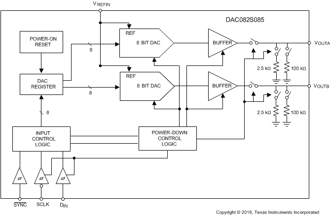
The DAC082S085 is fabricated on a CMOS process with an architecture that consists of switches and resistor strings that are followed by an output buffer.
8.2 Functional Block Diagram

8.2.1 Feature Description
8.2.1.1 DAC Architecture
The DAC082S085 is fabricated on a CMOS process with an architecture that consists of switches and resistor strings that are followed by an output buffer. The reference voltage is externally applied at VREFIN and is shared by both DACs.
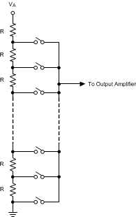
For simplicity, a single resistor string is shown in Figure 29. This string consists of 256 equal valued resistors with a switch at each junction of two resistors, plus a switch to ground. The code loaded into the DAC register determines which switch is closed, connecting the proper node to the amplifier. The input coding is straight binary with an ideal output voltage calculated in Equation 1:
where
- D is the decimal equivalent of the binary code that is loaded into the DAC register. (D can take on any value between 0 and 255. This configuration ensures that the DAC is monotonic.)
 Figure 29. DAC Resistor String
8.2.1.2 Output Amplifiers
The output amplifiers are rail-to-rail, providing an output voltage range of 0 V to VA when the reference is VA. All amplifiers, even rail-to-rail types, exhibit a loss of linearity as the output approaches the supply rails (0 V and VA, in this case). For this reason, linearity is specified over less than the full output range of the DAC. However, if the reference is less than VA, there is only a loss in linearity in the lowest codes. The output capabilities of the amplifier are described in Electrical Characteristics.
The output amplifiers are capable of driving a load of 2 kΩ in parallel with 1500 pF to ground or to VA. The zero-code and full-scale outputs for given load currents are available in the Electrical Characteristics.
8.2.1.3 Reference Voltage
The DAC082S085 uses a single external reference that is shared by both channels. The reference pin, VREFIN, is not buffered and has an input impedance of 60 kΩ. TI recommends that VREFIN be driven by a voltage source with low output impedance. The reference voltage range is 1 V to VA, providing the widest possible output dynamic range.
8.2.1.4 Power-On Reset
The power-on reset circuit controls the output voltages of both DACs during power-up. Upon application of power, the DAC registers are filled with zeros and the output voltages are 0 V. The outputs remain at 0 V until a valid write sequence is made to the DAC.
8.3 Device Functional Modes
8.3.1 Power-Down Modes
The DAC082S085 has four power-down modes, two of which are identical. In power-down mode, the supply current drops to 20 µA at 3 V and 30 µA at 5 V. The DAC082S085 is set in power-down mode by setting OP1 and OP0 to 11. Because this mode powers down both DACs, the first two bits of the shift register are used to select different output terminations for the DAC outputs. Setting A1 and A0 to 00 or 11 causes the outputs to be tri-stated (a high impedance state). While setting A1 and A0 to 01 or 10 causes the outputs to be terminated by 2.5 kΩ or 100 kΩ to ground respectively (see Table 1).
Table 1. Power-Down Modes
| A1 | A0 | OP1 | OP0 | OPERATING MODE |
|---|---|---|---|---|
| 0 | 0 | 1 | 1 | High-Z outputs |
| 0 | 1 | 1 | 1 | 2.5 kΩ to GND |
| 1 | 0 | 1 | 1 | 100 kΩ to GND |
| 1 | 1 | 1 | 1 | High-Z outputs |
The bias generator, output amplifiers, resistor strings, and other linear circuitry are all shut down in any of the power-down modes. However, the contents of the DAC registers are unaffected when in power-down. Each DAC register maintains its value prior to the DAC082S085 being powered down unless it is changed during the write sequence which instructed it to recover from power down. Minimum power consumption is achieved in the power-down mode with SYNC and DIN idled low and SCLK disabled. The time to exit power-down (Wake-Up Time) is typically tWU µs as stated in Timing Requirements.
8.4 Programming
8.4.1 Serial Interface
The three-wire interface is compatible with SPI™, QSPI, and MICROWIRE, as well as most DSPs and operates at clock rates up to 40 MHz. See Figure 1 for information on a write sequence.
A write sequence begins by bringing the SYNC line low. Once SYNC is low, the data on the DIN line is clocked into the 16-bit serial input register on the falling edges of SCLK. To avoid misclocking data into the shift register, it is critical that SYNC not be brought low simultaneously with a falling edge of SCLK (see Figure 1). On the 16th falling clock edge, the last data bit is clocked in and the programmed function (a change in the DAC channel address, mode of operation or register contents) is executed. At this point the SYNC line may be kept low or brought high. Any data and clock pusles after the 16th falling clock edge are ignored. In either case, SYNC must be brought high for the minimum specified time before the next write sequence is initiated with a falling edge of SYNC.
Because the SYNC and DIN buffers draw more current when they are high, they must be idled low between write sequences to minimize power consumption.
8.4.2 Input Shift Register
The input shift register, Figure 30, has sixteen bits. The first bit must be set to 0 and the second bit is an address bit. The address bit determines whether the register data is for DAC A or DAC B. This bit is followed by two bits that determine the mode of operation (writing to a DAC register without updating the outputs of both DACs, writing to a DAC register and updating the outputs of both DACs, writing to the register of both DACs and updating their outputs, or powering down both outputs). The final twelve bits of the shift register are the data bits. The data format is straight binary (MSB first, LSB last), with all 0s corresponding to an output of 0 V and all 1s corresponding to a full-scale output of VREFIN – 1 LSB. The contents of the serial input register are transferred to the DAC register on the sixteenth falling edge of SCLK. See Figure 1.
 Figure 30. Input Register Contents
Normally, the SYNC line is kept low for at least 16 falling edges of SCLK and the DAC is updated on the 16th SCLK falling edge. However, if SYNC is brought high before the 16th falling edge, the data transfer to the shift register is aborted and the write sequence is invalid. Under this condition, the DAC register is not updated and there is no change in the mode of operation or in the DAC output voltages.
8.4.3 DSP and Microprocessor Interfacing
Interfacing the DAC082S085 to microprocessors and DSPs is quite simple. The following guidelines are offered to hasten the design process.
8.4.3.1 ADSP-2101/ADSP2103 Interfacing
Figure 31 shows a serial interface between the DAC082S085 and the ADSP-2101/ADSP2103. The DSP must be set to operate in the SPORT Transmit Alternate Framing Mode. It is programmed through the SPORT control register and must be configured for Internal Clock Operation, Active Low Framing and 16-bit Word Length. Transmission is started by writing a word to the TX register after the SPORT mode has been enabled.
 Figure 31. ADSP-2101/2103 Interface
8.4.3.2 80C51/80L51 Interface
A serial interface between the DAC082S085 and the 80C51/80L51 microcontroller is shown in Figure 32. The SYNC signal comes from a bit-programmable pin on the microcontroller. The example shown here uses port line P3.3. This line is taken low when data is transmitted to the DAC082S085. Because the 80C51/80L51 transmits
8-bit bytes, only eight falling clock edges occur in the transmit cycle. To load data into the DAC, the P3.3 line must be left low after the first eight bits are transmitted. A second write cycle is initiated to transmit the second byte of data, after which port line P3.3 is brought high. The 80C51/80L51 transmit routine must recognize that the 80C51/80L51 transmits data with the LSB first while the DAC082S085 requires data with the MSB first.
 Figure 32. 80C51/80L51 Interface
8.4.3.3 68HC11 Interface
A serial interface between the DAC082S085 and the 68HC11 microcontroller is shown in Figure 33. The SYNC line of the DAC082S085 is driven from a port line (PC7 in the figure), similar to the 80C51/80L51.
The 68HC11 must be configured with its CPOL bit as a zero and its CPHA bit as a one. This configuration causes data on the MOSI output to be valid on the falling edge of SCLK. PC7 is taken low to transmit data to the DAC. The 68HC11 transmits data in 8-bit bytes with eight falling clock edges. Data is transmitted with the MSB first. PC7 must remain low after the first eight bits are transferred. A second write cycle is initiated to transmit the second byte of data to the DAC, after which PC7 must be raised to end the write sequence.
 Figure 33. 68HC11 Interface
8.4.3.4 Microwire Interface
Figure 34 shows an interface between a Microwire-compatible device and the DAC082S085. Data is clocked out on the rising edges of the SK signal. As a result, the SK of the Microwire device must be inverted before driving the SCLK of the DAC082S085.
 Figure 34. Microwire Interface