ZHCSDM6A JUNE 2013 – December 2014 DAC161S997
PRODUCTION DATA.
- 1 特性
- 2 应用
- 3 说明
- 4 简化电路原理图
- 5 修订历史记录
- 6 Pin Configuration and Functions
- 7 Specifications
- 8 Detailed Description
- 9 Application and Implementation
- 10Power Supply Recommendations
- 11Layout
- 12器件和文档支持
- 13机械、封装和可订购信息
8 Detailed Description
8.1 Overview
The DAC161S997 is a 16-bit DAC realized as a ∑Δ modulator. The DAC’s output is a current pulse train that is filtered by the on-board low pass RC filter. The final output current is a multiplied copy of the filtered modulator output. This architecture ensures an excellent linearity performance, while minimizing power consumption of the device.
The DAC161S997 eases the design of robust, precise, long-term stable industrial systems by integrating all precision elements on-chip. Only a few external components are needed to realize a low-power, high-precision industrial 4 - 20 mA transmitter.
In case of a fault, or during initial power-up the DAC161S997 will output current in either upper or lower error current band. The choice of band is user selectable via a device pin. The error current value is user programmable via SPI.
8.2 Functional Block Diagram
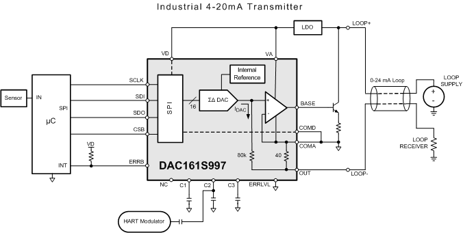
8.3 Feature Description
8.3.1 Error Detection And Reporting
By default, the DAC161S997 detects and reports several types of errors.
8.3.1.1 Loop Error
A loop error occurs when the device is unable to sustain the required output current at OUT pin, typically caused by a drop in loop supply, or an increase in load impedance.
When a loop error occurs, the DAC161S997 changes the OUT-pin current to the value in the ERROR_LOW register, unless the MASK_LOOP_ERR is set to 1. If the MASK_LOOP_ERR is not set, then the device also periodically attempts to reassert the OUT current set in DACCODE by default. If the DACCODE-current output is set, the DAC161S997 then stops reporting a loop error. The interval between reasserts is controlled by the L_RETRY_TIME field in the ERROR_CONFIG register. If the DIS_RETRY_LOOP field in the ERROR_CONFIG register is changed to 1, the device does not periodically check the loop and, instead, only checks the loop after a read of the ERR_STATUS (0x09) register. If the loop error is not resolved, then the loop-error current persists.
When a loop error occurs, the DAC161S997 sets the CURR_LOOP_STATUS and LOOP_STATUS fields in the STATUS register to 1. The LOOP_STATUS field remains set to 1 until the STATUS register is read or the device is reset. If the loop error is cleared, either by the device reasserting the loop current or by changing the OUT current , then the CURR_LOOP_STATUS field clears.
8.3.1.2 SPI Timeout Error (Channel Error)
The DAC161S997 expects to receive periodic SPI write commands to ensure that the SPI connection is functioning normally. If no SPI write command occurs within the time indicated by the SPI_TIMEOUT field in the ERROR_CONFIG register, the device reports a SPI timeout error. Note that the SPI write command must be properly formatted to avoid SPI Timeout errors (such as a write command that generates a frame error does not prevent an imminent SPI Timeout error).
SPI Timeout error reporting is inhibited by MASK_SPI_TOUT. SPI Timeout errors are not reported on the loop if MASK_SPI_ERR is set to 1.
Note that a write command to address 0 is not considered a valid write command and will not prevent a SPI Timeout error.
8.3.1.3 Frame Error
If a SPI write command has an incorrect number of SCLK pulses, the device reports a frame error. The number of SCLK pulses must be an integer and a multiple of 24. A frame error is always reported by ERRB being pulled low. A frame error does not affect the loop current.
8.3.1.4 Alarm Current
By default, the DAC161S997 reports faults to the plant controller by forcing the OUT current into one of two error bands. The error current bands are defined as either greater than 20 mA, or less than 4 mA. Loop errors are reported by setting current of ERR_LOW.
If SPI Timeout Errors are reported on the loop (this is the default; it can be changed by setting the register ERR_CONFIG:MASK_LOOP_ERR), the error band is controlled by the ERRLVL pin. When ERRLVL is tied to the COMD voltage, the ERR_LOW current is the reporting current. If ERRLVL is tied to VD then the ERR_HIGH current is the current-on pin, OUT, if a SPI timeout error occurs.
The exact value of the output current used to indicate fault is dictated by the contents of ERR_HIGH and ERR_LOW registers.
In the case of a conflicting alarm-current setting (such as a loop error and SPI timeout error occurring simultaneously and ERRLVL is tied high), the current-on pin, OUT, is determined by ERR_LOW current.
8.4 Device Functional Modes
The DAC161S997 reports errors in 3 different ways, by changing the OUT pin current, pulling the ERRB pin low, and by updating the read-only register STATUS. The reporting on ERRB and OUT pin is customized by setting the ERROR_CONFIG register.
The ERRB pin connects to a GPIO pin on the microcontroller to function as an interrupt if an error occurs.
If a Loop error and a SPI Timeout error occur simultaneously and the device is configured with conflicting error output currents, the OUT pin current reports the Loop Error.
| STATUS Register | Loop Reporting | ERRB Reporting | |
|---|---|---|---|
| Frame Error | Reported in FERR_STS | Not reported | Always reported |
| Loop Error | Reported in LOOP_STS and CURR_LOOP_STS | Reported by default unless ERR_CONFIG:MASK_LOOP_ERR is set to 1 | Reported by default unless ERR_CONFIG:DIS_LOOP_ERR_ERRB is set to 1 |
| SPI Timeout Error | Reported in SPI_TIMEOUT_ERR | Reported by default unless either ERR_CONFIG:MASK_SPI_ERR or ERR_CONFIG:MASK_SPI_TOUT are set to 1 | Reported by default unless ERR_CONFIG:MASK_SPI_TOUT is set to 1 |
8.5 Programming
8.5.1 Serial Interface
The 4-wire interface is compatible with SPI, QSPI, and MICROWIRE, as well as most DSPs. See the Timing Requirements section for timing information about the read and write sequences. The serial interface is comprised of CSB, SCLK, SDIs and SDO. The DAC161S997 supports both Mode 0 and Mode 3 of the SPI protocol.
A bus transaction is initiated by the falling edge of CSB. When CSB is low, the input data is sampled at the SDI pin by the rising edge of the SCLK. The output data is asserted on the SDO pin at the falling edge of SCLK.
A valid transfer requires an integer multiple of 24 SCLK cycles. If CSB is raised before the 24th rising edge of the SCLK, the transfer aborts and a Frame Error is reported. If CSB is held low after the 24th falling edge of the SCLK and additional SCLK edges occur, the data continues to flow through the FIFO and out the SDO pin. When CSB transitions high, the internal controller decodes the most recent 24 bits that were received before the rising edge of CSB. CSB must transition to high after an integer multiple of 24 clock cycles, otherwise a Frame Error is reported and the transaction is considered invalid. When a valid number of SCLK pulses occur with CSB low, the DAC then performs the requested operation after CSB transitions high.
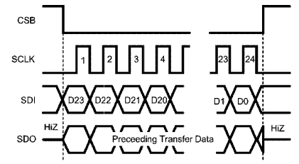 Figure 8. SPI Data Format
The acquired data is shifted into an internal 24-bit shift register (MSB first) which is configured as a 24-bit deep FIFO. As the data is being shifted into the FIFO via the SDI pin, the prior contents of the register are being shifted out through the SDO output. While CSB is high, SDO is in a high Z-state. At the falling edge of CSB, SDO presents the MSB of the data present in the shift register. SDO is updated on every subsequent falling edge of SCLK.
NOTE
The first SDO transition will happen on the first falling edge AFTER the first rising edge of SCLK when CSB is low.
The 24 bits of data contained in the FIFO are interpreted as an 8-bit COMMAND word followed by 16-bits of DATA. The general format of the 24-bit data stream is shown in Figure 9. Complete instruction set is tabulated in the Detailed Description section.
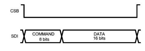 Figure 9. SPI Command and Data Words
8.5.1.1 SPI Write
SPI write operation is used to change the state of the device. Handshaking does not occur between the master and the slave (DAC161S997), and the master must control the communication on the following inputs: SCLK, CSB, SDI. The format of the data transfer is described in the Serial Interface section.
A write is composed of two sections, 8-bits corresponding to a command and 16-bits of data. A command is simply the address of the desired register to update. Note that some registers are read-only; a write to these registers will have no effect on the device operation and the register contents will not change. The user instruction set is shown in the Detailed Description section.
During power up or device reset, the register contents of all writable registers are set to the listed values in the Detailed Description section.
If the DAC161S997 is used in a highly noisy environment in which SPI errors are potentially an issue, the DAC161S997 supports a more robust protocol (see Optional Protected SPI Writes).
8.5.1.2 SPI Read
The read operation requires all 4 wires of the SPI interface, which are SCLK, SCB, SDI, and SDO. The simplest READ operation occurs automatically during any valid transaction on the SPI bus because the SDO pin of DAC161S997 always shifts out the contents of the internal FIFO. Therefore the data being shifted in to the FIFO is verified by initiating another transaction and acquiring data at SDO, allowing only for the verification of FIFO contents.
The internal registers are accessed by the user through a register read command. A register read command is formed by setting bit 7 of the command to 1 (effectively ORing with 0x80) with the address of the desired register to be read and sending the resulting 8 bits as the command (see Detailed Description). For example, the register read command of the STATUS register (address 0x05) would be 0x85.
A register read requires two SPI transactions to recover the register data. The first transaction shifts in the register read command; an 8-bits of command byte followed by 16-bits of dummy data. The register read command transfers the contents of the internal register into the FIFO. The second transaction shifts out the FIFO contents; an 8-bit command byte (which is a copy of previous transaction) followed by the register data. The Register Read operation is shown in Figure 10.
 Figure 10. SPI Register Read Operation
8.5.1.3 Optional Protected SPI Writes
The DAC161S997 supports an optional SPI protocol intended to provide robust support against SPI write errors.
When PROTECT_REG_WR is set to 1, all register writes require a subsequent XFER_REG command (a write of 0x00FF to XFER_REG[0x01]) to load the transferred data into the register address (see Figure 11). This requirement provides protection against write errors in an electrically noisy environment.
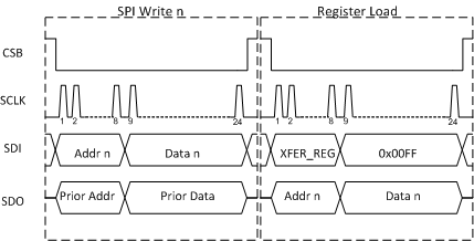 Figure 11. Protected SPI writes
8.5.1.3.1 SPI Write Error Correction
To minimize the chance of a SPI write error, TI recommends to append a NOP command onto the end of every register write sequence to verify that the XFER_REG is properly executed, as shown in Figure 12.
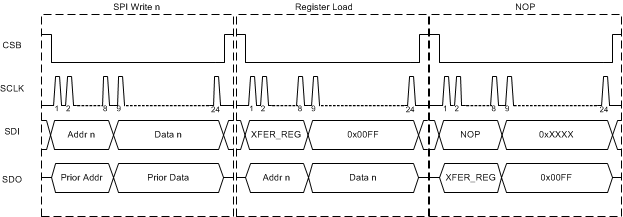 Figure 12. Protected SPI writes with NOP command
The XFER_REG command combined with the automatic SDO loopback of the previous SPI write data prevents loading of incorrect data into a register. If the loopback indicates a communication error has occurred (see Figure 13), the CSB pin is held low and the previous write command is repeated. Although the second SPI transaction had 48 SCLK pulses instead of 24 pulses, this is not considered a frame error. A frame error is indicated when the number of SCLK pulses is not an integer multiple of 24.
 Figure 13. Detection of Error in Register Load
If a communication error occurs in the XFER_REG command, it is detected during the trailing NOP command (see Figure 14). Although the register load is incomplete, the device has not changed operations. Repeat the original data and XFER_REG command.
 Figure 14. Detection of Error in Register Readback
8.6 Register Maps
Unless otherwise indicated, bits outside the register fields listed below are do not care, and will not change device configuration. Register read operations on such do not care fields will be 0. Registers are read/write unless indicated otherwise.
Table 1. XFER_REG (Write Only)
| Address = 0x01 | ||||
|---|---|---|---|---|
| Bit Field | Field Name | Description | ||
| 15:0 | XFER[15:0] | When PROTECT_REG_WR is set to 1, then a XFER_REG command is necessary to transfer the previous register write data into the appropriate address. Set this register to 0x00FF to perform a XFER_REG command. | ||
Table 2. NOP
| Address = 0x02 | ||||
|---|---|---|---|---|
| Bit Field | Field Name | Description | ||
| 15:0 | NOP[15:0] | No Operation. A write to this register will not change any device configuration. | ||
| This command indicates that the SPI connection is functioning and is used to avoid SPI_INACTIVE errors. | ||||
Table 3. WR_MODE
| Address = 0x03; Default = 0x0000 | ||||
|---|---|---|---|---|
| Bit Field | Field Name | Description | ||
| 0 | PROTECT_REG_WR | 0: Register write data transfers to appropriate address immediately after CSB goes high. Default value. | ||
| 1: Enable protected register transfers: all register writes require a subsequent XFER_REG command to finalize the loading of register data. Refer to Optional Protected SPI Writes. | ||||
Table 4. DACCODE
| Address = 0x04; Default = 0x2400, 0xE800 | ||||
|---|---|---|---|---|
| Bit Field | Field Name | Description | ||
| 15:0 | DACCODE[15:0] | 16-bit natural binary word, where D15 is the MSB, which indicates the desired DAC output code. | ||
| Note the default value of this register is based on the state of the ERR_LVL pin during startup or reset. | ||||
Table 5. ERR_CONFIG
| Address = 0x05; Default = 0x0102 | ||||
|---|---|---|---|---|
| Bit Field | Field Name | Description | ||
| 10:8 | L_RETRY_TIME[2:0] | L_RETRY_TIME sets the time interval between successive attempts to reassert the desired DACCODE output current when a loop error is present. This has no effect if either MASK_LOOP_ERR is set to 1 or if DIS_RETRY_LOOP is set to 1. | ||
| LOOP Retry time = (L_RETRY_TIME + 1) × 50 ms | ||||
| Default value = 1 (100 ms) | ||||
| 7 | DIS_RETRY_LOOP | 0: When a loop error is occurring, periodically attempt to send desired DACCODE output current instead of the set ERR_LOW current. The interval between attempts is set by L_RETRY_TIMER. Default value. | ||
| 1: Do not periodically reassert DACCODE output when a loop error is present; reassert DACCODE after STATUS Register is read out. | ||||
| 6 | MASK_LOOP_ERR | 0: When a LOOP error is detected the DAC161S997 outputs the current indicated by ERR_LOW instead of DACCCODE. Default value. | ||
| 1: When a Loop Error is detected the DAC161S997 tries to maintain DACCODE current on pin OUT. | ||||
| 5 | DIS_LOOP_ERR_ERRB | 0: When a LOOP error is detected the DAC161S997 drives ERRB pin low. Default value. | ||
| 1: When a LOOP error is detected the DAC161S997 does not drive ERRB pin low. | ||||
| 4 | MASK_SPI_ERR | 0: SPI timeout errors change the OUT pin current to an error value, which is determined by ERRLVL pin and contents of ERR_LOW or ERR_HIGH. Note: MASK_SPI_TOUT must be set to 0 for this to be reported. Default value. | ||
| 1: SPI timeout errors do not change the OUT pin current to an error value. | ||||
| 3:1 | SPI_TIMEOUT[2:0] | SPI_TIMEOUT sets the time interval for SPI timeout error reporting. After each SPI write command, an internal timer is reset; if no subsequent write occurs before the timer reaches SPI timeout, a SPI timeout error is reported. SPI_ERROR reporting is inhibited by setting MASK_SPI_TOUT. | ||
| A NOP write is considered a valid write and resets the timer without changing the device configuration. | ||||
| SPI Timeout = (SPI_TIMEOUT + 1) × 50 ms | ||||
| SPI_TIMEOUT default value = 1 (100 ms) | ||||
| 0 | MASK_SPI_TOUT | 0: SPI timeout error reporting is enabled. A SPI timeout error drives ERRB low when a SPI Timeout error occurs. Default value. | ||
| 1: SPI timeout error reporting is inhibited. | ||||
Table 6. ERR_LOW
| Address = 0x06; Default = 0x2400 | ||||
|---|---|---|---|---|
| Bit Field | Field Name | Description | ||
| 15:8 | ERR_LOW[7:0] | Under some error conditions the output current corresponding to this value is the DAC output, regardless of the value of DACCODE. The ERR_LOW value is used as the upper byte of the DACCODE, while the lower byte is forced to 0x00. | ||
| ERR_LOW must be between 0x00(0 mA) and 0x80(12 mA). The DAC161S997 ignores any value outside of that range and retains the previous value in the register. Refer to the Error Detection And Reporting section for additional details. | ||||
| The default value is 0x24, which corresponds to approximately 3.37 mA on pin OUT. | ||||
Table 7. ERR_HIGH
| Address = 0x07; Default = 0xE800 | ||||
|---|---|---|---|---|
| Bit Field | Field Name | Description | ||
| 15:8 | ERR_HIGH[7:0] | Under some error conditions the output current corresponding to this value is the DAC output, regardless of the value of DACCODE. The ERR_HIGH value is used as the upper byte of the DACCODE, while the lower byte is forced to 0x00. | ||
| ERR_HIGH must be greater than or equal to 0x80 (12 mA). The DAC161S997 ignores any value below 0x80 and retains the previous value in the register. Refer to the Error Detection And Reporting section for additional details. | ||||
| The default value is 0xE8, which corresponds to approximately 21.8 mA on pin OUT. | ||||
Table 8. RESET
| Address = 0x08 | ||||
|---|---|---|---|---|
| Bit Field | Field Name | Description | ||
| 15:0 | RESET[15:0] | Write 0xC33C to the RESET register followed by a NOP to reset the device. All writable registers are returned to default values. | ||
Table 9. STATUS (Read-Only)
| Address = 0x09 or 0x7F | ||||
|---|---|---|---|---|
| Bit Field | Field Name | Description | ||
| 7:5 | DAC_RES[2:0] | DAC resolution | ||
| On DAC161S997, returns a 111. | ||||
| 4 | ERRLVL_PIN | Returns the state of the ERRLVL pin: | ||
| 1 = ERRLVL pin is tied HIGH | ||||
| 0 = ERRLVL pin is tied LOW | ||||
| 3 | FERR_STS | Frame-error status sticky bit | ||
| 1 = A frame error has occurred since the last STATUS read. | ||||
| 0 = No frame error occurred since the last STATUS read. | ||||
| This error is cleared by reading the STATUS register. A frame error is caused by an incorrect number of clocks during a register write. A register write without an integer multiple of 24 clock cycles will cause a Frame error. | ||||
| 2 | SPI_TIMEOUT_ERR | SPI time out error | ||
| 1 = The SPI interface has not received a valid command within the interval set by SPI_TIMEOUT. | ||||
| 0 = The SPI interface has received a valid command within the interval set by SPI_TIMEOUT | ||||
| If this error occurs, it is cleared with a properly formatted write command to a valid address. | ||||
| 1 | LOOP_STS | Loop status sticky bit | ||
| 1 = A loop error has occurred since last read of STATUS. | ||||
| 0 = No loop error has occurred since last read of STATUS. | ||||
| Returns the loop error status. When the value in this register is 1, the DAC161S997 is unable to maintain the output current set by DACCODE at some point since the last STATUS read. This indicator clears after reading the STATUS register. | ||||
| 0 | CURR_LOOP_STS | Current loop status | ||
| 1 = A loop error is occurring. | ||||
| 0 = No loop error is occurring. | ||||
| Returns the current Loop error status. When the value in this register is 1, the DAC161S997 is unable to maintain the output current set by DACCODE. | ||||