ZHCSDM6A JUNE 2013 – December 2014 DAC161S997
PRODUCTION DATA.
- 1 特性
- 2 应用
- 3 说明
- 4 简化电路原理图
- 5 修订历史记录
- 6 Pin Configuration and Functions
- 7 Specifications
- 8 Detailed Description
- 9 Application and Implementation
- 10Power Supply Recommendations
- 11Layout
- 12器件和文档支持
- 13机械、封装和可订购信息
9 Application and Implementation
NOTE
Information in the following applications sections is not part of the TI component specification, and TI does not warrant its accuracy or completeness. TI’s customers are responsible for determining suitability of components for their purposes. Customers should validate and test their design implementation to confirm system functionality.
9.1 Application Information
9.1.1 16-bit Dac And Loop Drive
9.1.1.1 DC Characteristics
The DAC converts the 16-bit input code in the DACCODE registers to an equivalent current output. The ΣΔ DAC output is a current pulse which is then filtered by a third-order RC lowpass filter and boosted to produce the loop current (ILOOP) at the device OUT pin.
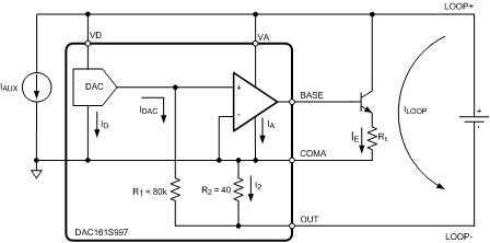 Figure 15. Loop-Powered Transmitter
Figure 15 shows the principle of operation of the DAC161S997 in the Loop-Powered Transmitter (the circuit details are omitted for clarity). In Figure 15, ID and IA represent supply (quiescent) currents of the internal digital and analog blocks. IAUX represents supply (quiescent) current of companion devices present in the system, such as the voltage regulator and the digital interface. Because both the control loop formed by the amplifier and the bipolar transistor force the voltage across R1 and R2 to be equal, under normal conditions, the ILOOP is dependent only on IDAC through the following relationship (see Equation 1).
where
- IDAC = ƒ(DACCODE)
Although ILoop has a number of component currents, ILOOP = IDAC + ID + IA + IAUX + IE, only IE is regulated by the loop to maintain the relationship shown in Equation 1. Because only the magnitude of IE is controlled, not the direction, there is a lower limit to ILOOP. This limit is dependent on the fixed components IA and ID, and on system implementation through IAUX.
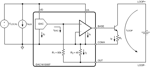 Figure 16. Self-Powered Transmitter
Figure 16 shows the variant of the transmitter where the local supply provides supply currents to the system blocks, and not the 4-20mA loop Self-Powered Transmitter. The ame basic relationship between the ILOOP and IDAC continues, but the component currents of ILOOP are only IDAC and IE.
9.1.1.2 DC Input-Output Transfer Function
The output current sourced by the OUT pin of the device is expressed by Equation 2.
The valid DACCODE range is the full 16-bit code space (0x0000 to 0xFFFF), resulting in the IDAC range of 0 to approximately 12 μA, which, however, does not result in the ILOOP range of 0 to 24 mA. The maximum output current sourced out of OUT pin, ILOOP, is 24 mA. The minimum output current is dependent on the system implementation. The minimum output current is the sum of the supply currents of the DAC161S997 internal blocks, IA, ID, and companion devices present in the system, IAUX. The last component current, IE, is theoretically controlled down to 0, however, due to the stability considerations of the control loop, not allowing the IE to drop below 200 μA is advised.
The graph in Figure 17 shows the DC transfer characteristic of the 4-20mA transmitter, including minimum current limits. The minimum current limit for the Loop-Powered Transmitter is typically around 400 μA (ID+ IA + IAUX + IE). The minimum current limit for the Self-Powered Transmitter is typically around 200 μA (IE). Typical values for ID and IA are listed in the Electrical Characteristics table. IE depends on the BJT device used.
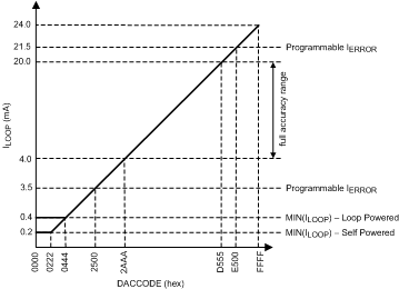 Figure 17. DAC-DC Transfer Function
9.1.1.3 Loop Interface
The DAC161S997 cannot directly interface to the typical 4 - 20 mA loop due to the excessive loop supply voltage. The loop interface has to provide the means of stepping down the LOOP Supply to 3.6V. This can be accomplished with either a linear regulator (LDO) or switching regulator while keeping in mind that the regulator’s quiescent current will have direct effect on the minimum achievable ILOOP (see DC Input-Output Transfer Function).
The second component of the loop interface is the external NPN transistor (BJT). This device is part of the control circuit that regulates the transmitter’s output current (ILOOP). Since the BJT operates over the wide current range, spanning at least 4 - 20 mA, it is necessary to degenerate the emitter in order to stabilize transistor’s transconductance (gm). The degeneration resistor of 22Ω is suggested in typical applications. For circuit details, see Figure 21.
The NPN BJT should not be replaced with an N-channel FET (Field Effect Transistor) for the following reasons: discrete FET’s typically have high threshold voltages (VT), in the order of 1.5V to 2V, which is beyond the BASE output maximum range; discrete FET’s present higher load capacitance which may degrade system stability margins; and BASE output relies on the BJT’s base current for biasing.
9.1.1.4 Loop Compliance
The maximum V(LOOP+,LOOP-) potential is limited by the choice of step-down regulator, and the external BJT’s Collector Emitter breakdown voltage. For minimum V(LOOP+, LOOP−) potential consider TROUBLE Figure 16. Here, observe that V(LOOP+,LOOP−) ≅ min(VCE) + ILOOPRE + ILOOPR2 = min(VCE) + 0.53V + 0.96V = 3.66V, at ILOOP = 24mA. The voltage drop across internal R2 is specified in Electrical Characteristics.
9.1.1.5 AC Characteristics
The approximate frequency dependent characteristics of the loop drive circuit can be analyzed using the circuit in Figure 18.
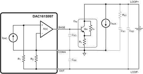 Figure 18. Capacitances Affecting Control Loop
Here it is assumed that the internal amplifier dominates the frequency response of the system, and it has a single pole response. The BJT’s response, in the bandwidth of the control loop, is assumed to be frequency independent and is characterized by the transconductance gm and the output resistance ro.
As in previous sections IDAC and IAUX represent the filtered output of the ∑Δ modulator and the quiescent current of the companion devices.
The circuit in Figure 18 can be further simplified by omitting the on-board capacitances, whose effect will be discussed in Stability, and by combining the amplifier, the external transistor and resistor RE into one Gm block. The resulting circuit is shown in Figure 19.
By assuming that the BJT’s output resistance (ro) is large, the loop current ILOOP can be expressed as:

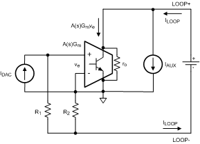 Figure 19. AC Analysis Model of a Transmitter
The sum of voltage drops around the path containing R1, R2 and ve is:

An assumption is made on the response of the internal amplifier:

By combining the above the final expression for the ILOOP as a function of 2 inputs IDAC and IAUX is:
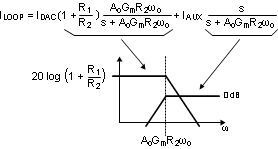
The result above reveals that there are 2 distinct paths from the inputs IDAC and IAUX to the output ILOOP. IDAC follows the low-pass, and the IAUX follows the high-pass path.
In both cases the corner frequency is dependent on the effective transconductance, Gm, of the external transistor. This implies that control loop dynamics could vary with the output current ILOOP if Gm were allowed to be just native device transconductance gm. This undesirable behavior is mitigated by the degenerating resistor RE which stabilizes Gm as follows:
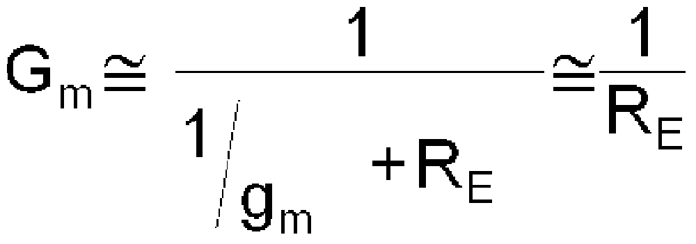
This results in the frequency response which is largely independent of the output current ILOOP:

While the bandwidth of the IDAC path may not be of great consequence given the low frequency nature of the 4-20 mA current loop systems, the location of the pole in the IAUX path directly affects PSRR of the transmitter circuit. This is further discussed in PSRR.
9.1.1.5.1 Step Response
The transient input-output characteristics of the DAC161S997 are dominated by the response of the RC filter at the output of the ∑Δ DAC. Settling times due to step input are shown in Typical Characteristics.
9.1.1.5.2 Output Impedance
The output impedance is described as:

By considering the circuit in Figure 19, and setting IDAC = IAUX = 0, the following expression can be obtained:

As in AC Characteristics an assumption can be made on the frequency response of the internal amplifier, and the effective transconductance Gm should be stabilized with external RE leading to:
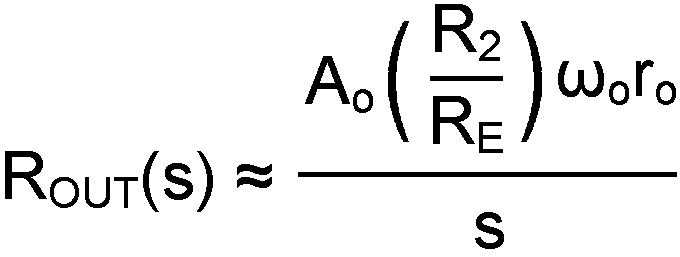
The output impedance of the transmitter is a product of the external BJT's output resistance ro, and the frequency characteristics of the internal amplifier. At low frequencies this results in a large impedance that does not significantly affect the output current accuracy.
9.1.1.5.3 PSRR
Power Supply Rejection Ratio is defined as the ability of the current control loop to reject the variations in the supply current of the companion devices, IAUX. Specifically:

It was shown in AC Characteristics that the IAUX affects ILOOP via the high-pass path whose corner frequency is dependent on the effective Gm of the external BJT. If that dependence were not mitigated with the degenerating resistor RE, the PSRR would be degraded at low output current ILOOP.
The typical PSRR performance of the transmitter shown in Figure 6 is shown in Typical Characteristics.
9.1.1.5.4 Stability
The current control loop's stability is affected by the impedances present in the system. Figure 18 shows the simplified diagram of the control loop, formed by the on-board amplifier and an external BJT, and the lumped capacitances CX1 through CX4 that model any other external elements.
CX1 typically represents a local step-down regulator, or LDO, and any other companion devices powered from the LOOP+. This capacitance reduces the stability margins of the control loop, and therefore it should be limited. RX1 can be used to isolate CX1 from LOOP+ node and thus remedy the stability margin reduction. If RX1 = 0, CX1 cannot exceed 10 nF. RX1 = 200Ω is recommended if it can be tolerated. Minimum RX1 = 40Ω if CX1 exceeds 10 nF.
CX3 also adversely affects stability of the loop and it must be limited to 20 pF. CX4 affects the control loop in the same way as CX1, and it should be treated in the same way as CX1. CX2 is the only capacitance that improves stability margins of the control loop. Its maximum size is limited only by the safety requirements.
Stability is a function of ILOOP as well. Since ILOOP is approximately equal to the collector current of the external BJT, Gm of the BJT, and thus loop dynamics, depend on ILOOP. This dependence can be reduced by degenerating the emitter of the BJT with a small resistance as discussed in Loop Interface. Inductance in series with the LOOP+ and LOOP− do not significantly affect the control loop.
9.1.1.5.5 Noise and Ripple
The output of the DAC is a current pulse train. The transition density varies throughout the DAC input code range (ILOOP range). At the extremes of the code range, the transition density is the lowest which results in low frequency components of the DAC output passing through the RC filter. Hence, the magnitude of the ripple present in ILOOP is the highest at the ends of the transfer characteristic of the device (see Typical Characteristics).
It should be noted that at wide noise measurement bandwidth, it is the ripple due to the ∑Δ modulator that dominates the noise performance of the device throughout the entire code range of the DAC. This results in the “U” shaped noise characteristic as a function of output current. At narrow bandwidths, and particularly at mid-scale output currents, it is the amplifier driving the external BJT that starts to dominate as a noise source.
9.1.1.5.6 Digital Feedthrough
Digital feedthrough is indiscernible from the ripple induced by the ∑Δ modulator.
9.1.1.5.7 HART Signal Injection
The HART specification requires minimum suppression of the sensor signal in the HART signal band (1-2 kHz) of about 60 dB. The filter in Figure 20 below meets that requirement.
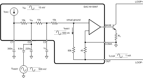 Figure 20. HART Signal Injection
9.1.1.5.8 RC Filter Limitation
In an effort to speed up the transient response of the device the user can reduce the capacitances associated with the low-pass filter at the output of the ∑Δ modulator. However, to maintain stability margins of the current control loop it is necessary to have at least C1 = C2 = C3 = 1nF.
9.2 Typical Application
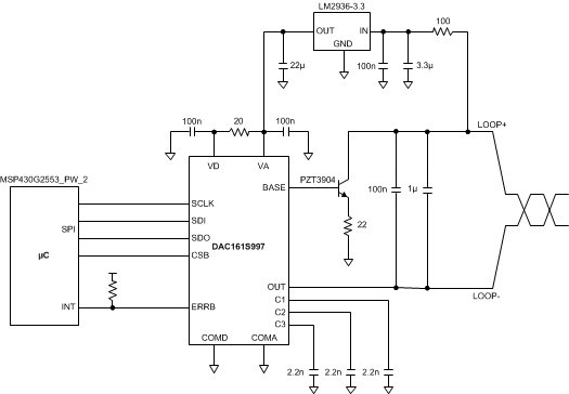 Figure 21. Typical Application Schematic
9.2.1 Design Requirements
The objective of the example below is to focus on the design of a robust, low-power, precise, long- term stable, 2-wire, loop-powered, 4- to 20-mA current-output temperature transmitter by making best use of signal chain, power and computing solutions. This design uses a RTD-temperature sensor with a 4- to 20-mA current-loop transmitter.
9.2.2 Detailed Design Procedure
The DAC161S997output is a current pulse which is then filtered by a third-order RC low-pass filter and boosted to produce the loop current (ILOOP) at the device OUT pin. Figure 22 shows the principle of operation of the DAC161S997 in the loop-powered transmitter. The ILOOP has a number of component currents as given in Equation 13.

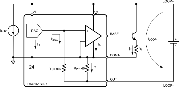 Figure 22. Loop Powered Transmitter
9.2.2.1 Reasons for Choosing a 3.9-V Zener Diode
The first and most important requirement for the proper functioning of the entire circuitry is a stable power supply. A good design ensures that the LDO gets the sufficient input voltage (VIN_LDO) to generate a stable 3.3 V under minimum-loop, power-supply voltage and minimum-loop current conditions.
From the circuit implementation, it is evident that the LDO input voltage VIN_LDO is function of loop current and collector-emitter drop (VCE ) of the bipolar junction transistor (BJT). Apply Kirchhoff ’ s Voltage Law (KVL) in the inner loop:
At minimum loop power supply voltage, BJT operation is pushed towards saturation, which means that VCE is approximately 0 V (minimum). Due to the stability considerations of the current control loop, the minimum output current (ILOOP(MIN)) below 200 μ A is not advised as shown in Figure 23.
To ensure stable 3.3-V LDO output under these conditions, the following relation must be fulfilled.
[(100 Ω × 200 μA)+ VZENER + 0 V + (20 Ω X 200 μA)] > 3.4 V
[VZENER + 0.024 V] > 3.4 V
From Equation 17, it is clear that without having a zener diode, a voltage greater than 3.4 V at the input of the LDO cannot be ensured. Therefore, choose a zener diode having a zener voltage (VZENER) greater than 3.4 V and able to handle power dissipation, PDZ = VZENER × ILOOP(MAX). In this application, the design uses a 3.9-V, 500-mW zener diode.
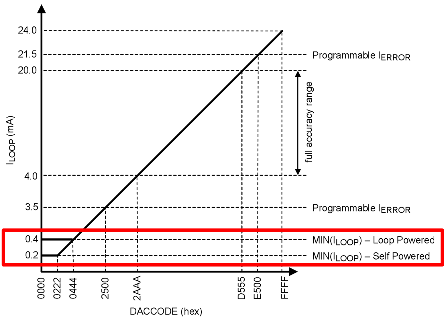 Figure 23. DAC DC Transfer Function
9.2.2.2 Loop Compliance Voltage
To calculate the minimum-loop, compliance-voltage (loop-power supply voltage), add all voltage drops in the loop at the maximum-expected loop current.
From a current control loop stability point of view, VCE(MIN) must stay greater than maximum VCE(SAT):
Applying Kirchhoff ’s Voltage Law in the outer loop, to find out the VCE(MIN):
where
- 2 × VWIRE is voltage drop across system wiring. If system wiring runs over a length (L) along one way, wire resistance per unit length is ρ and current in the loop is ILOOP, then the voltage drop for one conductor can be given as:
- VWIRE(MAX) = ρ × L × ILOOP(MAX)
- For example, a 24-AWG wire has resistance per unit length ( ρ ) of 0.026 Ω /ft or 0.0755 Ω /m.
- VLOAD is the voltage drop caused by the internal resistance of the loop receiver. The internal resistance of the loop receiver may vary from 50 Ω to 250 Ω .
- VLOAD(MAX) = RLOAD × ILOOP(MAX)
- VSENSE is the voltage drop across 40- Ω sense resistor internal to the DAC.
- VF is the forward-voltage drop across the reverse polarity protection diode.
- VF = 0.7 V at 30 mA forward current (from TVS data sheet, SM6T39CA Data Sheet,SM6T39CA).
Rewriting Equation 19,
The maximum output current that can be sourced out of the OUT pin by DAC161S997, I LOOP (MAX) , is approximately 24 mA.
 Figure 24. Series Voltage Drops in Current Loop System
 Figure 25. Specification for Loop Current Output
Next, examine what NAMUR NE43 has to say about loop current. NAMUR NE43 is an international association of process instrumentation user companies that have worked on improving the diagnostic coverage in 4- to 20-mA analog output transmitters to address associated safety issues. NAMUR NE43 provides the guideline for signaling-failure information to the safety-interlock systems over a 4- to 20-mA loop. NAMUR NE43 recommends using 3.8 mA to 20.5 mA as an extended measurement information range. NAMUR NE43 recommends using loop current below 3.6 mA or above 21 mA is in the diagnostic failure information range. Choose ILOOP(MAX) = 24 mA, depending upon DAC capability and also to comply with the NAMUR NE43 recommendation as shown in Figure 26.
 Figure 26. NAMUR NE43 Recommendation
Rewriting Equation 20,
Figure 27 and Figure 28 give the loop supply voltages calculated using Equation 22 at different receiver load resistances and system wiring lengths.
 Figure 27. Loop Power Supply Voltage for Different Loads and System Wiring Length in Feet
 Figure 28. Loop Power Supply Voltage for Different Loads and System Wiring Length in Meter
However, the maximum loop compliance voltage must not exceed the absolute maximum voltage rating of any device used in the loop. Therefore, select the device in order to meet the maximum loop compliance voltage requirement
9.2.2.3 Selection of External BJT
DAC161S997 has been designed to use an external NPN transistor (BJT). Transistor Q1 conducts the majority of the signal-dependent, 4-20mA loop current. Using an external transistor avoids on-chip power dissipation and thermally-induced errors. Since the external transistor is part of a current control loop, the external transistor characteristics are not critical. Virtually any transistor with sufficient voltage, current and, power rating may be used. Basic requirements are as follows:
- VCEO = 40 V minimum
- β = 40 minimum
- Must be able to handle power dissipation, PD = VCE(MAX) × ILOOP(MAX)
The NPN BJT should not be replaced with an N-channel Field Effect Transistor (FET) for the following reasons. Discrete FET ’ s typically have high threshold voltages (VTH), in the order of 1.5 V to 2 V, which is beyond the BASE output maximum range. Discrete FETs present higher load capacitance, which may degrade system stability margins. BASE output relies on the BJT’s base current for biasing.
For further information on a complete reference design of a Small Form Factor, 2-Wire, 4- to 20-mA Current-Loop, RTD Temperature Transmitter, refer to TIDU385A.
9.2.3 Application Curve
Unless otherwise noted, these specifications apply for VA = VD = 3.3 V, COMA = COMD = 0 V, TA= 25°C, external bipolar transistor: 2N3904, RE = 22 Ω, C1 = C2 = C3 = 2.2 nF.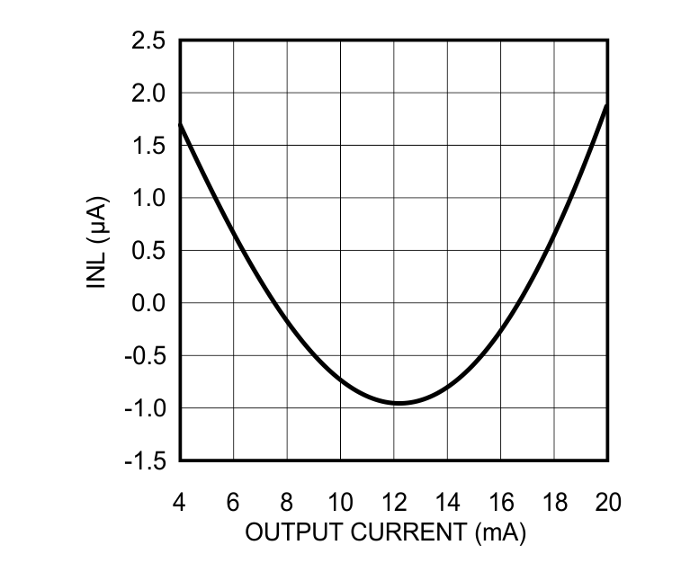 Figure 29. Linearity vs ILOOP