ZHCS964E February 2012 – September 2015 DAC34SH84
PRODUCTION DATA.
- 1 特性
- 2 应用范围
- 3 说明
- 4 修订历史记录
- 5 Pin Configuration and Functions
-
6 Specifications
- 6.1 Absolute Maximum Ratings
- 6.2 ESD Ratings
- 6.3 Recommended Operating Conditions
- 6.4 Thermal Information
- 6.5 Electrical Characteristics - DC Specifications
- 6.6 Electrical Characteristics - Digital Specifications
- 6.7 Electrical Characteristics - AC Specifications
- 6.8 Timing Requirements - Digital Specifications
- 6.9 Switching Characteristics - AC Specifications
- 6.10 Typical Characteristics
-
7 Detailed Description
- 7.1 Overview
- 7.2 Functional Block Diagram
- 7.3
Feature Description
- 7.3.1 Serial Interface
- 7.3.2 Data Interface
- 7.3.3 Data Format
- 7.3.4 Input FIFO
- 7.3.5 FIFO Modes of Operation
- 7.3.6 Clocking Modes
- 7.3.7 FIR Filters
- 7.3.8 Complex Signal Mixer
- 7.3.9 Quadrature Modulation Correction (QMC)
- 7.3.10 Temperature Sensor
- 7.3.11 Data Pattern Checker
- 7.3.12 Parity Check Test
- 7.3.13 DAC34SH84 Alarm Monitoring
- 7.3.14 LVPECL Inputs
- 7.3.15 LVDS Inputs
- 7.3.16 CMOS Digital Inputs
- 7.3.17 Reference Operation
- 7.3.18 DAC Transfer Function
- 7.3.19 Analog Current Outputs
- 7.4 Device Functional Modes
- 7.5 Programming
- 7.6 Register Map
- 8 Application and Implementation
- 9 Power Supply Recommendations
- 10Layout
- 11器件和文档支持
- 12机械、封装和可订购信息
8 Application and Implementation
NOTE
Information in the following applications sections is not part of the TI component specification, and TI does not warrant its accuracy or completeness. TI’s customers are responsible for determining suitability of components for their purposes. Customers should validate and test their design implementation to confirm system functionality.
8.1 Application Information
The DAC34SH84 is a dual 16-bit DAC with max input data rate of up to 750 MSPS per DAC and max DAC update rate of 1.5 GSPS after the final, selectable interpolation stages. With build-in interpolation filter of 2x, 4x, 8x, and 16x options, the lower input data rate can be interpolated all the way to 1.5 GSPS. This allows the DAC to update the samples at higher rate, and pushes the DAC images further away to relax anti-image filer specification due to the increased Nyquist bandwidth. With integrated coarse and fine mixers, baseband signal can be upconverted to an intermediate frequency (IF) signal between the baseband processor and post-DAC analog signal chains.
The DAC can output baseband or IF when connected to post-DAC analog signals chain components such as transformers or IF amplifiers. When used in conjunction with TI RF quadrature modulator such as the TRF3705, the DAC and RF modulator can function as a set of baseband or IF upconverter. With integrated QMC circuits, the LO offset and the sideband artifacts can be properly corrected in the direct up-conversion applications. The DAC34SH84 provides the bandwidth, performance, small footprint, and lower power consumption needed for multi-mode 2G/3G/4G cellular base stations to migrate to more advanced technologies, such as LTE-Advanced and carrier aggregation on multiple antennas.
8.2 Typical Applications
8.2.1 IF Based LTE Transmitter
Figure 88 shows an example block diagram for a direct conversion radio. The design requires a single carrier, 20-MHz LTE signal. The system has digital-predication (DPD) to correct up to 5th order distortion so the total DAC output bandwidth is 100 MHz. Interpolation is used to output the signal at highest sampling rate possible to simplify the analog filter requirements and move high order harmonics out of band (due to wider Nyquist zone). The internal PLL is used to generate the final DAC output clock from a reference clock of 491.52 MHz.
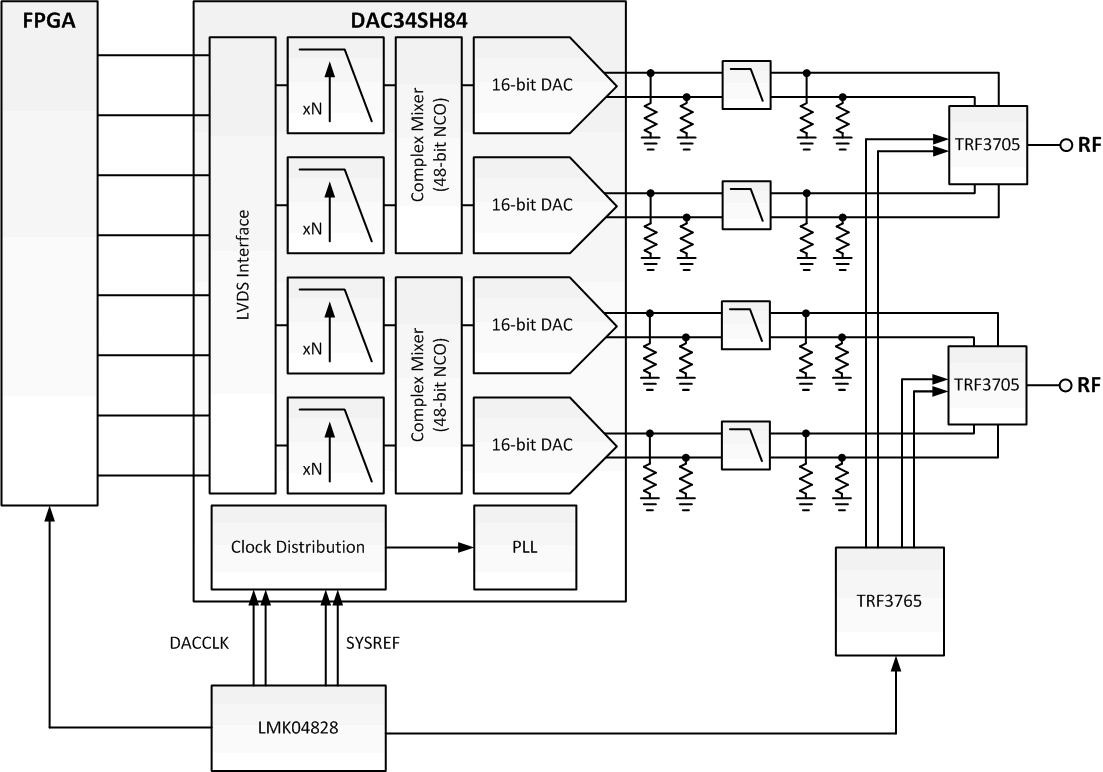 Figure 88. Dual Low-IF Wideband LTE Transmitter Diagram
8.2.1.1 Design Requirements
For this design example, use the parameters listed in Table 62 as the input parameters.
Table 62. Design Parameters
| DESIGN PARAMETER | EXAMPLE VALUE |
|---|---|
| Signal Bandwidth (BWsignal) | 20 MHz |
| Total DAC Output Bandwidth (BWtotal) | 100 MHz |
| DAC PLL | On |
| DAC PLL Reference Frequency | 491.52 MHz |
| Maximum FPGA LVDS Rate | 491.52 Mbps |
8.2.1.2 Detailed Design Procedure
8.2.1.2.1 Data Input Rate
Nyquist theory states that the data rate must be at least two times the highest signal frequency. The data will be sent to the DAC as complex baseband data. Due to the quadrature nature of the signal, each in-phase (I component) and quadrature (Q component) need to have 50 MHz of bandwidth to construct 100 MHz of complex bandwidth. Since the interpolation filter design is not the ideal half-band filter design with infinite roll-off at FDATA/2 (refer to FIR Filters section for more detail), the filter limits the useable input bandwidth to about 40 percent of FDATA. Therefore, the minimum data input rate is 125 MSPS. Since the standard telecom data rate is typically multiples of 30.72 MSPS, the DAC input data rate is chosen to be eight times of 30.72 MSPS, which is 245.76 MSPS.
8.2.1.2.2 Interpolation
It is desired to use the highest DAC output rate as possible to move the DAC images further from the signal of interest to ease analog filter requirement. The DAC output rate must be greater than two times the highest output frequency of 200 MHz, which is greater than 400 MHz. Table 63 shows the possible DAC output rates based on the data input rate and available interpolation settings. The DAC image frequency is also listed.
Table 63. Interpolation
| FDATA | INTERPOLATION | FDAC | POSSIBLE? | LOWEST IMAGE FREQUENCY | DISTANCE FROM BAND OF INTEREST |
|---|---|---|---|---|---|
| 245.76 MSPS | 1 | 245.76 MSPS | No | N/A | N/A |
| 245.76 MSPS | 2 | 491.52 MSPS | Yes | 318.64 MHz | 145.76 MHz |
| 245.76 MSPS | 4 | 983.04 MSPS | Yes | 810.16 MHz | 637.28 MHz |
| 245.76 MSPS | 8 | 1966.08 MSPS | No | N/A | N/A |
| 245.76 MSPS | 16 | 3932.16 MSPS | No | N/A | N/A |
8.2.1.2.3 LO Feedthrough and Sideband Correction
For typical IF based systems, the IF location is selected such that the image location and the LO feedthrough location is far from the signal location. The minimum distance is based on the bandpass filter roll-off and attenuation level at the LO feedthrough and image location. If sufficient attenuation level of these two artifacts meets the system requirement, then further digital cancellation of these artifacts may not be needed.
Although the I/Q modulation process will inherently reduce the level of the RF sideband signal, an IF based transmitter without sufficient RF image rejection capabilities or an zero-IF based system (detail in the next section) will likely need additional sideband suppression to maximize performance. Further, any mixing process will result in some feedthrough of the LO source. The DAC34SH84 has build-in digital features to cancel both the LO feedthrough and sideband signal. The LO feedthrough is corrected by adding a DC offset to the DAC outputs until the LO feedthrough power is suppressed. The sideband suppression can be improved by correcting the gain and phase differences between the I and Q analog outputs through the digital QMC block. Besides gain and phase differences between the I and Q analog outputs, group delay differences may also be present in the signal path and are typically contributed by group delay variations of post DAC image reject analog filters and PCB trace variations. Since delay in time translates to higher order linear phase variation, the sideband of a wideband system may not be completely suppressed by typical digital QMC block. The system designer may implement additional linear group delay compensation in the host processor to the DAC to perform higher order sideband suppression.
8.2.1.3 Application Curves
The ACPR performance for LTE 20 MHz TM1.1 are shown in Figure 89, Figure 90, Figure 90, and Figure 90. The figures provide comparisons between two major LTE bands such as 2.14 GHz and 2.655 GHz, and also comparisons between two different DAC clocking options such as DAC on-chip PLL mode and external clocking mode.
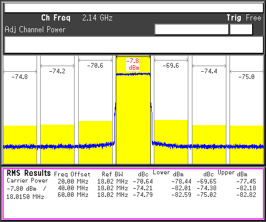
| DAC Output IF = 122.88 MHz, LO = 2017.12 MHz, DAC Clock = External Clock Source from LMK04806 |
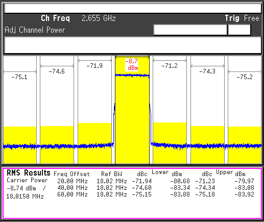
| DAC Output IF = 122.88 MHz, LO = 2532.12 MHz, DAC Clock = External Clock Source from LMK04806 |
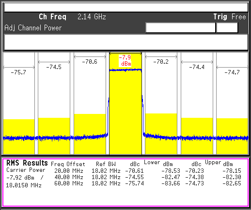
| DAC Output IF = 122.88 MHz, LO = 2017.12 MHz, DAC Clock = DAC34SH84 On-Chip PLL |
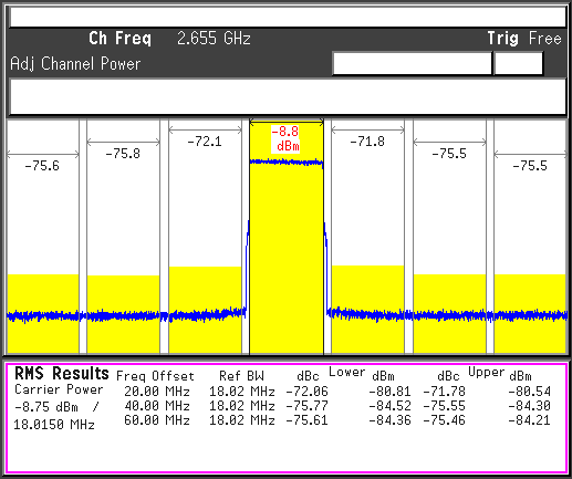
| DAC Output IF = 122.88 MHz, LO = 2532.12 MHz, DAC Clock = DAC34SH84 On-Chip PLL |
8.2.2 Direct Upconversion (Zero IF) LTE Transmitter
Figure 88 shows an example block diagram for a direct conversion radio. The design specification requires that the desired output bandwidth is 100 MHz, which could be, for instance, a typical LTE signal. The system has DPD to correct up to 5th order distortion so the total DAC output bandwidth is 500 MHz. Interpolation is used to output the signal at the highest sampling rate possible to simplify the analog filtering requirements and move high order harmonics out of band (due to wider Nyquist zone). The DAC sampling clock is provided by high quality clock synthesizer such as the LMK0480x family.
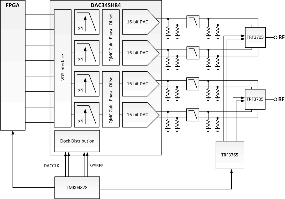 Figure 93. Zero LTE Transmitter Diagram
8.2.2.1 Design Requirements
For this design example, use the parameters listed in Table 64 as the input parameters.
Table 64. Design Parameters
| DESIGN PARAMETER | EXAMPLE VALUE |
|---|---|
| Signal Bandwidth (BWsignal) | 100 MHz |
| Total DAC Output Bandwidth (BWtotal) | 500 MHz |
| DAC PLL | Off |
| Maximum FPGA LVDS Rate | 1228.8 Mbps |
8.2.2.2 Detailed Design Procedure
8.2.2.2.1 Data Input Rate
Nyquist theory states that the data rate must be at least two times the highest signal frequency. The data will be sent to the DAC as complex baseband data. Due to the quadrature nature of the signal, each in-phase (I component) and quadrature (Q component) need to have 250 MHz of bandwidth to construct 500 MHz of complex bandwidth. Since the interpolation filter design is not the ideal half-band filter design with infinite roll-off at FDATA/2 (refer to FIR Filters section for more detail), the filter limits the useable input bandwidth to about 44 percent of FDATA with less than 0.1dB of FIR filter roll-off. Therefore, the minimum data input rate is 568 MSPS. Since the standard telecom data rate is typically multiples of 30.72 MSPS, the DAC input data rate is chosen to be 20 times of 30.72 MSPS, which is 614.4 MSPS. For the DAC34SH84, input data rate of 737.28 MSPS may also be used to meet additional bandwidth demand. This particular setting requires higher speed grade ASIC/FPGA that supports LVDS bus rate of 1474.56 Mbps minimum.
8.2.2.2.2 Interpolation
It is desired to use the highest DAC output rate as possible to move the DAC images further from the signal of interest to ease analog filter requirement. The DAC output rate must be greater than two times the highest output frequency of 250 MHz, which is greater than 500 MHz. The table below shows the possible DAC output rates based on the data input rate and available interpolation settings. The DAC image frequency is also listed.
Table 65. Interpolation
| FDATA | INTERPOLATION | FDAC | POSSIBLE? | LOWEST IMAGE FREQUENCY | DISTANCE FROM BAND OF INTEREST |
|---|---|---|---|---|---|
| 614.4 MSPS | 1 | 614.4 MSPS | Yes | 364.4 MHz | 114.4 MHz |
| 614.4 MSPS | 2 | 1228.8 MSPS | Yes | 978.8 MHz | 728.8 MHz |
| 614.4 MSPS | 4 | 2457.6 MSPS | No | N/A | N/A |
| 614.4 MSPS | 8 | 4915.2 MSPS | No | N/A | N/A |
| 614.4 MSPS | 16 | 9830.4 MSPS | No | N/A | N/A |
8.2.2.2.3 LO Feedthrough and Sideband Correction
Refer to LO Feedthrough and Sideband Correction section of IF based LTE Transmitter design.
8.2.2.3 Application Curves
The ACPR performance for LTE 20MHz TM1.1 are shown in Figure 94 and Figure 95. The figures provide comparisons between two major LTE bands such as 2.14 GHz and 2.655 GHz with DAC clocking option set to external clocking mode.
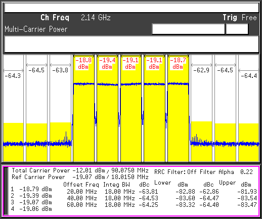
| DAC Output IF = 0 MHz, LO = 2140 MHz, DAC Clock = External Clock Source from LMK04806 |
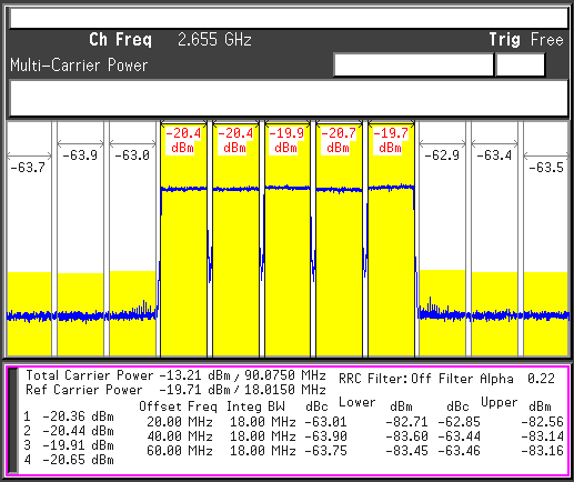
| DAC Output IF = 0 MHz, LO = 2655 MHz, DAC Clock = External Clock Source from LMK04806 |