ZHCSGG0B February 2017 – July 2017 DAC38RF86 , DAC38RF87 , DAC38RF96 , DAC38RF97
PRODUCTION DATA.
- 1 特性
- 2 应用
- 3 说明
- 4 修订历史记录
- 5 Device Comparison Table
- 6 Pin Configuration and Functions
-
7 Specifications
- 7.1 Absolute Maximum Ratings
- 7.2 ESD Ratings
- 7.3 Recommended Operating Conditions
- 7.4 Thermal Information
- 7.5 Electrical Characteristics - DC Specifications
- 7.6 Electrical Characteristics - Digital Specifications
- 7.7 Electrical Characteristics - AC Specifications
- 7.8 PLL/VCO Electrical Characteristics
- 7.9 Timing Requirements
- 7.10 Typical Characteristics, DAC38RF86 and DAC38RF96
-
8 Detailed Description
- 8.1 Overview
- 8.2 Functional Block Diagrams
- 8.3
Feature Description
- 8.3.1 SerDes Inputs
- 8.3.2 SerDes Rate
- 8.3.3 SerDes PLL
- 8.3.4 SerDes Equalizer
- 8.3.5 JESD204B Descrambler
- 8.3.6 JESD204B Frame Assembly
- 8.3.7 SYNC Interface
- 8.3.8 Single or Dual Link Configuration
- 8.3.9 Multi-Device Synchronization
- 8.3.10 SYSREF Capture Circuit
- 8.3.11 JESD204B Subclass 0 support
- 8.3.12 SerDes Test Modes through Serial Programming
- 8.3.13 SerDes Test Modes through IEEE 1500 Programming
- 8.3.14 Error Counter
- 8.3.15 Eye Scan
- 8.3.16 JESD204B Pattern Test
- 8.3.17 Multiband DUC (multi-DUC)
- 8.3.18 PA Protection Block
- 8.3.19 Gain Block
- 8.3.20 Output Summation
- 8.3.21 Output Delay
- 8.3.22 Polarity Inversion
- 8.3.23 Temperature Sensor
- 8.3.24 Alarm Monitoring
- 8.3.25 Differential Clock Inputs
- 8.3.26 CMOS Digital Inputs
- 8.3.27 DAC Fullscale Output Current
- 8.3.28 Current Steering DAC Architecture
- 8.3.29 DAC Transfer Function
- 8.4 Device Functional Modes
- 8.5
Register Maps
- 8.5.1 Chip Reset and Configuration Register (address = 0x00) [reset = 0x5803]
- 8.5.2 IO Configuration Register (address = 0x01) [reset = 0x1800]
- 8.5.3 Lane Single Detect Alarm Mask Register (address = 0x02) [reset = 0xFFFF]
- 8.5.4 Clock Alarms Mask Register (address = 0x03) [reset = 0xFFFF
- 8.5.5 SERDES Loss of Signal Detection Alarms Register (address = 0x04) [reset = 0x0000]
- 8.5.6 SYSREF Alignment Circuit Alarms Register (address = 0x05) [reset = 0x0000]
- 8.5.7 Temperature Sensor and PLL Loop Voltage Register (address = 0x06) [reset = variable]
- 8.5.8 Page Set Register (address = 0x09) [reset = 0x0000]
- 8.5.9 SYSREF Align to r1 and r3 Count Register (address = 0x78) [reset = 0x0000]
- 8.5.10 SYSREF Phase Count 1 and 2 Register (address = 0x79) [reset = 0x0000]
- 8.5.11 SYSREF Phase Count 3 and 4 Register (address = 0x7A) [reset = 0x0000]
- 8.5.12 Vendor ID and Chip Version Register (address = 0x7F) [reset = 0x0008]]
- 8.5.13 Multi-DUC Configuration (PAP, Interpolation) Register (address = 0x0A) [reset = 0x02B0]
- 8.5.14 Multi-DUC Configuration (Mixers) Register (address = 0x0C) [reset = 0x2402]
- 8.5.15 JESD FIFO Control Register (address = 0x0D) [reset = 0x1300]
- 8.5.16 Alarm Mask 1 Register (address = 0x0E) [reset = 0x00FF]
- 8.5.17 Alarm Mask 2 Register (address = 0x0F) [reset = 0xFFFF]
- 8.5.18 Alarm Mask 3 Register (address = 0x10) [reset = 0xFFFF]
- 8.5.19 Alarm Mask 4 Register (address = 0x11) [reset = 0xFFFF]
- 8.5.20 JESD Lane Skew Register (address = 0x12) [reset = 0x0000]
- 8.5.21 CMIX Configuration Register (address = 0x17) [reset = 0x0000]
- 8.5.22 Output Summation and Delay Register (address = 0x19) [reset = 0x0000]
- 8.5.23 NCO Phase Path AB Register (address = 0x1C) [reset = 0x0000]
- 8.5.24 NCO Phase Path CD Register (address = 0x1D) [reset = 0x0000]
- 8.5.25 NCO Frequency Path AB Register (address = 0x1E-0x20) [reset = 0x0000 0000 0000]
- 8.5.26 NCO Frequency Path CD Register (address = 0x21-0x23) [reset = 0x0000 0000 0000]
- 8.5.27 SYSREF Use for Clock Divider Register (address = 0x24) [reset = 0x0010]
- 8.5.28 Serdes Clock Control Register (address = 0x25) [reset = 0x7700]
- 8.5.29 Sync Source Control 1 Register (address = 0x27) [reset = 0x1144]
- 8.5.30 Sync Source Control 2 Register (address = 0x28) [reset = 0x0000]
- 8.5.31 PAP path AB Gain Attenuation Step Register (address = 0x29) [reset = 0x0000]
- 8.5.32 PAP path AB Wait Time Register (address = 0x2A) [reset = 0x0000]
- 8.5.33 PAP path CD Gain Attenuation Step Register (address = 0x2B) [reset = 0x0000]
- 8.5.34 PAP Path CD Wait Time Register (address = 0x2C) [reset = 0x0000]
- 8.5.35 PAP path AB Configuration Register (address = 0x2D) [reset = 0x0FFF]
- 8.5.36 PAP path CD Configuration Register (address = 0x2E) [reset = 0x0FFF]
- 8.5.37 DAC SPI Configuration Register (address = 0x2F) [reset = 0x0000]
- 8.5.38 DAC SPI Constant Register (address = 0x30) [reset = 0x0000]
- 8.5.39 Gain for path AB Register (address = 0x32) [reset = 0x0000]
- 8.5.40 Gain for path CD Register (address = 0x33) [reset = 0x0000]
- 8.5.41 JESD Error Counter Register (address = 0x41) [reset = 0x0000]
- 8.5.42 JESD ID 1 Register (address = 0x46) [reset = 0x0044]
- 8.5.43 JESD ID 2 Register (address = 0x47) [reset = 0x190A]
- 8.5.44 JESD ID 3 and Subclass Register (address = 0x48) [reset = 0x31C3]
- 8.5.45 JESD Lane Enable Register (address = 0x4A) [reset = 0x0003]
- 8.5.46 JESD RBD Buffer and Frame Octets Register (address = 0x4B) [reset = 0x1300]
- 8.5.47 JESD K and L Parameters Register (address = 0x4C) [reset = 0x1303]
- 8.5.48 JESD M and S Parameters Register (address = 0x4D) [reset = 0x0100]
- 8.5.49 JESD N, HD and SCR Parameters Register (address = 0x4E) [reset = 0x0F4F]
- 8.5.50 JESD Character Match and Other Register (address = 0x4F) [reset = 0x1CC1]
- 8.5.51 JESD Link Configuration Data Register (address = 0x50) [reset = 0x0000]
- 8.5.52 JESD Sync Request Register (address = 0x51) [reset = 0x00FF]
- 8.5.53 JESD Error Output Register (address = 0x52) [reset = 0x00FF]
- 8.5.54 JESD ILA Check 1 Register (address = 0x53) [reset = 0x0100]
- 8.5.55 JESD ILA Check 2 Register (address = 0x54) [reset = 0x8E60]
- 8.5.56 JESD SYSREF Mode Register (address = 0x5C) [reset = 0x0001]
- 8.5.57 JESD Crossbar Configuration 1 Register (address = 0x5F) [reset = 0x0123]
- 8.5.58 JESD Crossbar Configuration 2 Register (address = 0x60) [reset = 0x4567]
- 8.5.59 JESD Alarms for Lane 0 Register (address = 0x64) [reset = 0x0000]
- 8.5.60 JESD Alarms for Lane 1 Register (address = 0x65 01100101) [reset = 0x0000]
- 8.5.61 JESD Alarms for Lane 2 Register (address = 0x66) [reset = 0x0000]
- 8.5.62 JESD Alarms for Lane 3 Register (address = 0x67) [reset = 0x0000]
- 8.5.63 JESD Alarms for Lane 4 Register (address = 0x68) [reset = 0x0000]
- 8.5.64 JESD Alarms for Lane 5 Register (address = 0x69) [reset = 0x0000]
- 8.5.65 JESD Alarms for Lane 6 Register (address = 0x6A [reset = 0x0000]
- 8.5.66 JESD Alarms for Lane 7 Register (address = 0x6B) [reset = 0x0000]
- 8.5.67 SYSREF and PAP Alarms Register (address = 0x6C) [reset = 0x0000]
- 8.5.68 Clock Divider Alarms 1 Register (address = 0x6D) [reset = 0x0000]
- 8.5.69 Clock Configuration Register (address = 0x0A) [reset = 0xF000]
- 8.5.70 Sleep Configuration Register (address = 0x0B) [reset = 0x0022]
- 8.5.71 Divided Output Clock Configuration Register (address = 0x0C) [reset = 0x8000]
- 8.5.72 DAC Fullscale Current Register (address = 0x0D) [reset = 0xF000]
- 8.5.73 Internal SYSREF Generator Register (address = 0x10) [reset = 0x0000]
- 8.5.74 Counter for Internal SYSREF Generator Register (address = 0x11) [reset = 0x0000]
- 8.5.75 SPI SYSREF for Internal SYSREF Generator Register (address = 0x12) [reset = 0x0000]
- 8.5.76 Digital Test Signals Register (address = 0x1B) [reset = 0x0000]
- 8.5.77 Sleep Pin Control Register (address = 0x23) [reset = 0xFFFF]
- 8.5.78 SYSREF Capture Circuit Control Register (address = 0x24) [reset = 0x1000]
- 8.5.79 Clock Input and PLL Configuration Register (address = 0x31) [reset = 0x0200]
- 8.5.80 PLL Configuration 1 Register (address = 0x32) [reset = 0x0308]
- 8.5.81 PLL Configuration 2 Register (address = 0x33) [reset = 0x4018]
- 8.5.82 LVDS Output Configuration Register (address = 0x34) [reset = 0x0000]
- 8.5.83 Fuse Farm clock divider Register (address = 0x35) [reset = 0x0018]
- 8.5.84 Serdes Clock Configuration Register (address = 0x3B) [reset = 0x0002]
- 8.5.85 Serdes PLL Configuration Register (address = 0x3C) [reset = 0x8228]
- 8.5.86 Serdes Configuration 1 Register (address = 0x3D) [reset = 0x0x0088]
- 8.5.87 Serdes Configuration 2 Register (address = 0x3E) [reset = 0x0x0909]
- 8.5.88 Serdes Polarity Control Register (address = 0x3F) [reset = 0x0000]
- 8.5.89 JESD204B SYNCB OUTPUT Register (address = 0x76) [reset = 0x0000]
- 9 Application and Implementation
- 10Power Supply Recommendations
- 11Layout
- 12器件和文档支持
- 13机械、封装和可订购信息
9 Application and Implementation
NOTE
Information in the following applications sections is not part of the TI component specification, and TI does not warrant its accuracy or completeness. TI’s customers are responsible for determining suitability of components for their purposes. Customers should validate and test their design implementation to confirm system functionality.
9.1 Application Information
9.2 Typical Application: Multi-band Radio Frequency Transmitter
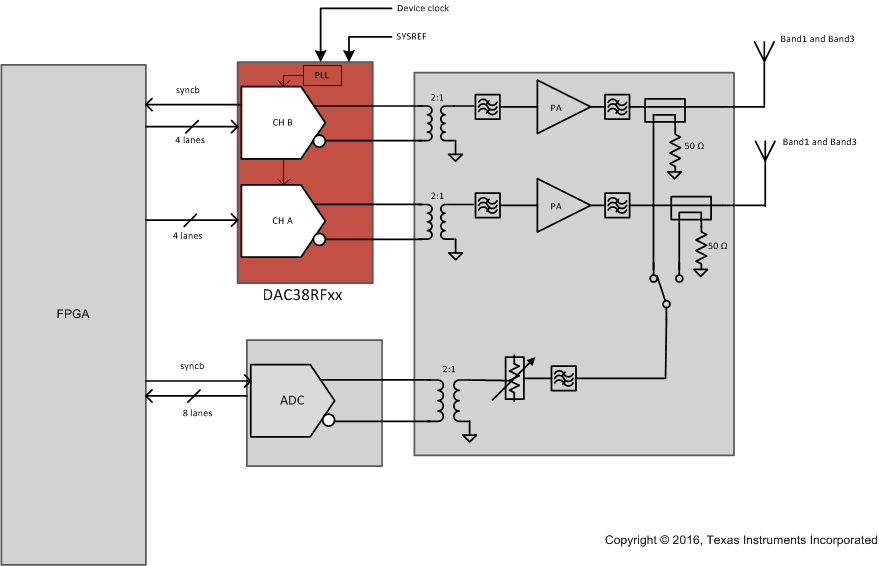
The DAC38RF8xx device family can be used in RF transmitters designed to support multiple operating bands. The two transmit antennae system shown in Figure 151 uses DAC38RF8xx to convert digital baseband signals from an FPGA directly to RF signals in LTE downlink band 1 (2110 MHz - 2170 MHz) and band 3 (1805 MHz - 1880 MHz).
 Figure 151. Two antennae multi-band Radio Frequency Transmitter
9.2.1 Design Requirements
Table 132. Dual band LTE downlink transmitter
| Parameter | Value |
|---|---|
| Operating bands | Band 1 (2110 MHz - 2170 MHz) and Band 3 (1805 MHz to 1880 MHz) |
| Data rate (baseband) | 368.64 MHz |
| Sampling frequency | 8847.36 MHz |
| Interpolation | 24 |
| JESD204B Interface configuration | L-M-F-S-Hd = 8-8-2-1-0 |
9.2.2 Detailed Design Procedure
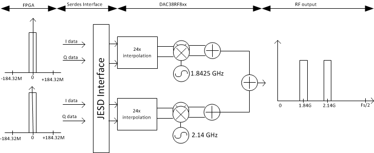
Two complex data streams of 20MHz LTE data generated in a baseband processor (FPGA/ASIC) is formatted based on Table 18and transmitted to DAC38RF8xx. Inside DAC38RF8xx, the complex input data at a rate of 368.64 MSPS is interpolated 24 times to the final output sampling rate of 8847.36 MSPS. This enables the final RF output to be positioned in the first Nyquist zone for minimal attenuation due to sinc(x) roll off. After interpolation, the output complex data stream is digitally mixed to the final RF frequencies. The digital mixing eliminates system imperfections such as local oscillator (LO) feed-through and sideband images that are inherent in analog mixers. Detailed block diagram is shown in (Figure 152)
To simplify the system clocking, a low frequency clock (or device clock) is provided as a reference to the on-chip PLL (Internal PLL/VCO) of DAC38RF8xx. The PLL generates a low phase noise, high frequency sampling clock from the low frequency reference.
 Figure 152. Dual band LTE Downlink Transmitter Block Diagram
9.2.2.1 Calculating the JESD204B SerDes Rate
SerDes rate = 1.25 x (M/L) x Baseband data rate x Number of bits per sample (16)
M is a JESD204B interface parameter that refers to the number of data streams from FPGA to DAC
L is a JESD204B interface parameter that refers to the number of SerDes lanes used to transmit data
1.25 is a factor due to the 8B10B encoding of the baseband data
Example,
if the baseband data rate = 368.64 MSPS and L-M-F-S-Hd = 8-8-2-1-0
9.2.2.2 Calculating valid JESD204B SYSREF Frequency
Valid SYSREF frequencies depend on the following parameters:
- Sample clock frequency
- JESD204B internal clock divider value (CLKJESD_DIV). This depends on the DAC JESD204B L-M-F-S mode and interpolation
- Number of octets in a frame (F)
- Number of frames in a multi-frame (K)
Maximum SYSREF frequency = (Sample clock frequency/N),
where N =LCM(CLKJESD_DIV,4 x K x F). N is the Least common multiple of 4 x K x F and CLKJESD_DIV.
All valid SYSREF frequencies are integer divisors of the maximum SYSREF frequency.
Example:
Given sampling clock frequency = 8.84736 GSPS, Interpolation = 24, DAC Mode=L-M-F-S=8-8-2-1 and K=20:
CLKJESD_DIV = 24 (CLKJESD_DIV)
Maximum SYSREF Frequency = 8847.36 MHz/240 = 36.864 MHz
Valid SYSREF Frequencies = 36.864 MHz/n, where n is any positive integer.
9.2.3 Application Curves
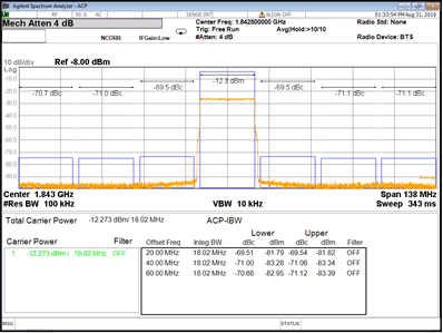
 Figure 153. Dual band ACPR Performance in Downlink Band 3 with On-chip PLL
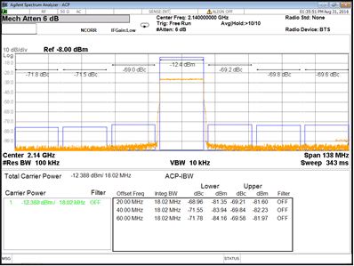
 Figure 154. Dual band ACPR Performance in Downlink Band 1 with On-chip PLL
