ZHCSLO2E October 2020 – January 2021 DAC5652
PRODUCTION DATA
- 1 特性
- 2 应用
- 3 说明
- 4 Revision History
- 5 Pin Configuration and Functions
-
6 Specifications
- 6.1 Absolute Maximum Rationgs
- 6.2 ESD Ratings
- 6.3 Recommended Operating Conditions
- 6.4 Thermal Resistance Characteristics
- 6.5 Electrical Characteristics
- 6.6 Electrical Characteristics
- 6.7 Electrical Characteristics, AC
- 6.8 Electrical Characteristics, DC
- 6.9 Switching Characteristics
- 6.10 Typical Characteristics
- 7 Parameter Measurement Information
- 8 Detailed Description
- 9 Application Information Disclaimer
- 10Power Supply Recommendations
- 11Layout
- 12Device and Documentation Support
- 13Mechanical, Packaging, and Orderable Information
8.3.2 Analog Outputs
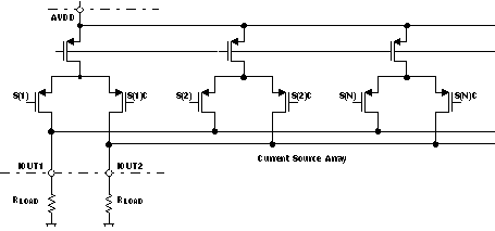
The DAC5652 provides two complementary current outputs, IOUT1 and IOUT2. The simplified circuit of the analog output stage representing the differential topology is shown in Figure 8-1. The output impedance of IOUT1 and IOUT2 results from the parallel combination of the differential switches, along with the current sources and associated parasitic capacitances.
 Figure 8-1 Analog
Outputs
Figure 8-1 Analog
OutputsThe signal voltage swing that may
develop at the two outputs, IOUT1 and IOUT2, is limited by a
negative and positive compliance. The negative limit of –1 V is given by the
breakdown voltage of the CMOS process and exceeding it compromises the reliability
of the DAC5652 (or even causes permanent damage). With the full-scale output set to
20 mA, the positive compliance equals 1.2 V. Note that the compliance range
decreases to about
1 V for a selected output current
of IOUTFS = 2 mA. Care must be taken that the configuration of DAC5652
does not exceed the compliance range to avoid degradation of the distortion
performance and integral linearity.
Best distortion performance is typically achieved with the maximum full-scale output signal limited to approximately 0.5 VPP. This is the case for a 50-Ω doubly-terminated load and a 20-mA full-scale output current. A variety of loads can be adapted to the output of the DAC5652 by selecting a suitable transformer while maintaining optimum voltage levels at IOUT1 and IOUT2. Furthermore, using the differential output configuration in combination with a transformer is instrumental for achieving excellent distortion performance. Common-mode errors, such as even-order harmonics or noise, can be substantially reduced. This is particularly the case with high output frequencies.
For those applications requiring the optimum distortion and noise performance, it is recommended to select a full-scale output of 20 mA. A lower full-scale range of 2 mA may be considered for applications that require low power consumption, but can tolerate a slight reduction in performance level.