ZHCSG81 April   2017 DCPA10505 , DCPA10505D , DCPA10512 , DCPA10512D , DCPA10515 , DCPA10515D

PRODUCTION DATA.  

  1. 特性
  2. 应用
  3. 说明
  4. 修订历史记录
  5. Pin Configuration and Functions
  6. Specifications
    1. 6.1  Absolute Maximum Ratings
    2. 6.2  ESD Ratings
    3. 6.3  Recommended Operating Conditions
    4. 6.4  Electrical Characteristics
    5. 6.5  Switching Characteristics
    6. 6.6  Typical Characteristics (DCPA10505)
    7. 6.7  Typical Characteristics (DCPA10512)
    8. 6.8  Typical Characteristics (DCPA10515)
    9. 6.9  Typical Characteristics (DCPA10505D)
    10. 6.10 Typical Characteristics (DCPA10512D)
    11. 6.11 Typical Characteristics (DCPA10515D)
  7. Detailed Description
    1. 7.1 Overview
    2. 7.2 Functional Block Diagrams
    3. 7.3 Feature Description
      1. 7.3.1  Isolation
        1. 7.3.1.1 Operation or Functional Isolation
        2. 7.3.1.2 Basic or Enhanced Isolation
        3. 7.3.1.3 Continuous Voltage
        4. 7.3.1.4 Isolation Voltage
        5. 7.3.1.5 Repeated High-Voltage Isolation Testing
      2. 7.3.2  Power Stage
      3. 7.3.3  Input and Output Capacitors
      4. 7.3.4  Oscillator And Watchdog Circuit
      5. 7.3.5  Synchronization
      6. 7.3.6  SWOUT
      7. 7.3.7  Soft Start
      8. 7.3.8  Load Regulation
      9. 7.3.9  Thermal Performance
        1. 7.3.9.1 Thermal Protection
      10. 7.3.10 Current Limit
      11. 7.3.11 Construction
  8. Application and Implementation
    1. 8.1 Application Information
      1. 8.1.1 Ripple Reduction
      2. 8.1.2 Connecting the DCPA1 in Series
      3. 8.1.3 Connecting the DCPA1 in Parallel
    2. 8.2 Typical Application
      1. 8.2.1 Design Requirements
      2. 8.2.2 DCPA10505 Application Curves
      3. 8.2.3 Detailed Design Procedure
        1. 8.2.3.1 Input Capacitor
        2. 8.2.3.2 Output Capacitor
        3. 8.2.3.3 SYNCIN Pin
      4. 8.2.4 PCB Design
  9. Power Supply Recommendations
  10. 10Layout
    1. 10.1 Layout Guidelines
    2. 10.2 Layout Example
  11. 11器件和文档支持
    1. 11.1 器件支持
      1. 11.1.1 器件命名规则
    2. 11.2 文档支持
      1. 11.2.1 相关文档
    3. 11.3 社区资源
    4. 11.4 相关链接
    5. 11.5 商标
    6. 11.6 静电放电警告
    7. 11.7 Glossary
  12. 12机械、封装和可订购信息

封装选项

机械数据 (封装 | 引脚)
散热焊盘机械数据 (封装 | 引脚)
订购信息

Specifications

Absolute Maximum Ratings

over operating free-air temperature range (unless otherwise noted) (1)
MIN MAX UNIT
Input voltage +VS –0.5 6 V
50ns transient –1.0 7 V
SYNCIN –0.5 +VS V
50ns transient –1.0 6 V
Lead temperature (soldering, 10 s) 260 °C
Storage temperature, Tstg –60 125 °C
Stresses beyond those listed under Absolute Maximum Ratings may cause permanent damage to the device. These are stress ratings only, which do not imply functional operation of the device at these or any other conditions beyond those indicated under Recommended Operating Conditions. Exposure to absolute-maximum-rated conditions for extended periods may affect device reliability.

ESD Ratings

VALUE UNIT
V(ESD) Electrostatic discharge Human-body model (HBM), per ANSI/ESDA/JEDEC JS-001 (1) ±1000 V
Charged-device model (CDM), per JEDEC specification JESD22-C101 (2) ±250
JEDEC document JEP155 states that 500-V HBM allows safe manufacturing with a standard ESD control process.
JEDEC document JEP157 states that 250-V CDM allows safe manufacturing with a standard ESD control process.

Recommended Operating Conditions

over operating free-air temperature range (unless otherwise noted)
MIN NOM MAX UNIT
Input voltage 4.5 5 5.5 V
Output power 0.05 1 W
Operating ambient temperature range –40 100 °C

Electrical Characteristics

TA = 25°C, +VS = nominal, CIN = 2.2 µF, COUT = 1.0 µF, (unless otherwise noted)
PARAMETER TEST CONDITIONS MIN TYP MAX UNIT
OUTPUT
POUT Output power Over +VS range, IOUT = 100% (full load) 1 W
IOUT Output current DCPA10505 200 mA
DCPA10505D 200(2) mA
DCPA10512 83 mA
DCPA10512D 83(2) mA
DCPA10515 66 mA
DCPA10515D 66(2) mA
VOUT Output voltage IOUT = 100% load (4) DCPA10505 5.0 V
DCPA10505D ±5.0 V
DCPA10512 12.0 V
DCPA10512D ±12.0 V
DCPA10515 15.0 V
DCPA10515D ±15.0 V
Temperature variation –40°C ≤ TA ≤ 100°C, IOUT = 100% load 0.02 %/°C
Line regulation +VS(MIN) to +VS(TYP), IOUT = 10% load 10%
+VS(TYP) to +VS(MAX), IOUT = 10% load 10%
Load regulation(1) 10% to 100% load 5%
VRIPPLE Output voltage ripple(5) COUT = 1 μF, IOUT = 50% 20 mVPP
INPUT
+VS Input voltage range 4.5 5.5 V
UVLO +VS Undervoltage lockout +VS increasing threshold 2.25 V
+VS decreasing threshold 1.7 V
IQ Quiescient current IOUT = 0% load DCPA10505 35 mA
DCPA10505D 25 mA
DCPA10512 29 mA
DCPA10512D 36 mA
DCPA10515 31 mA
DCPA10515D 38 mA
ISOLATION
VISO Isolation 1-second flash test, voltage DC 2.0(6)(5) kVDC
AC 1.5(6) kVrms
1-second flash test, leakage current 30 µA
Continuous working voltage across isolation barrier DC 60 VDC
AC 42.5 VAC
dV/dt 50 V/ms
CISO Barrier capacitance VISO = 750 Vrms 28 pF
PERFORMANCE
Efficiency IOUT = 100% DCPA10505 85%
DCPA10505D 85%
DCPA10512 87%
DCPA10512D 88%
DCPA10515 86%
DCPA10515D 86%
Transient response(5) 50% to 100% load step DCPA10505 3.0%
DCPA10512 1.9%
DCPA10515 2.0%
50% to 100% load step
per output(3)
DCPA10505D 2.7%
DCPA10512D 2.0%
DCPA10515D 1.6%
RELIABILITY
Demonstrated TA = 55°C 55 FITS
CAPACITANCE
CIN External input capacitance Ceramic 2.2 µF
COUT External output capacitance Ceramic 0.1 1.0 200 µF
THERMAL SHUTDOWN
TSD Die temperature at shutdown 168 °C
ISD Shutdown current 3 mA
Load regulation = (VOUT at 10% load – VOUT at 100%)/VOUT at 75% load
IOUT1 + IOUT2
Transient testing for dual output devices are tested with one output loaded with a 50% static load and the other output loaded with a 50% to 100% dynamic load step.
See Load Regulation graphs in the Typical Characterization section for typical voltage at all load conditions.
Guaranteed by design. Not production tested.
See Isolation Voltage section for more information.

Switching Characteristics

at TA = +25°C, +VS = nominal, CIN = 2.2 µF, COUT = 1.0 µF, (unless otherwise noted)
PARAMETER TEST CONDITIONS MIN TYP MAX UNIT
fOSC Oscillator frequency fSW = fOSC/2 850 kHz
fSYNC Synchronization frequency range 750 1000 kHz
VIH High-level input threshold, SYNCIN 0.7 V
VIL Low-level input threshold, SYNCIN 0.3 V

Typical Characteristics (DCPA10505)

At TA = 25°C, +VS = nominal, (unless otherwise noted)
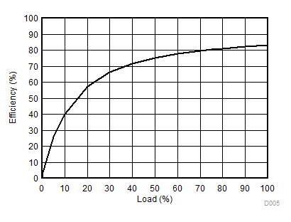
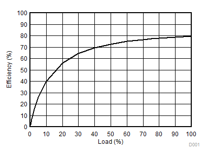
DCPA10505 DCPA10505D DCPA10512 DCPA10512D DCPA10515 DCPA10515D 5Veff.gif
DCPA10505
Figure 1. Efficiency vs Load
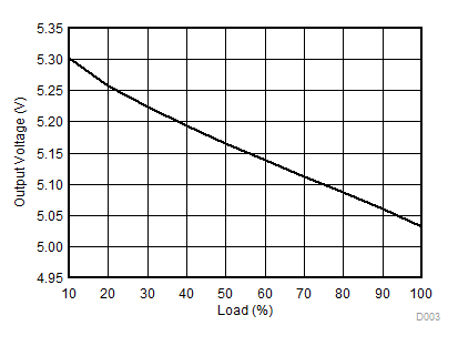
DCPA10505 DCPA10505D DCPA10512 DCPA10512D DCPA10515 DCPA10515D 5Vloadreg.gif
DCPA10505
Figure 3. Load Regulation
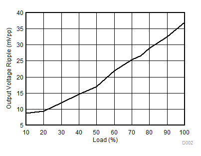
DCPA10505 DCPA10505D DCPA10512 DCPA10512D DCPA10515 DCPA10515D 5Vripple2.gif
DCPA10505 COUT = 1 µF
20-MHz BW
Figure 2. Output Ripple vs Load
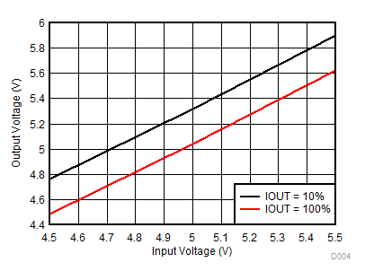
DCPA10505 DCPA10505D DCPA10512 DCPA10512D DCPA10515 DCPA10515D 5VlineReg2.gif
DCPA10505
Figure 4. Line Regulation

Typical Characteristics (DCPA10512)

At TA = 25°C, +VS = nominal, (unless otherwise noted)
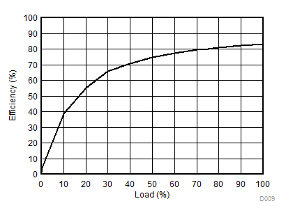
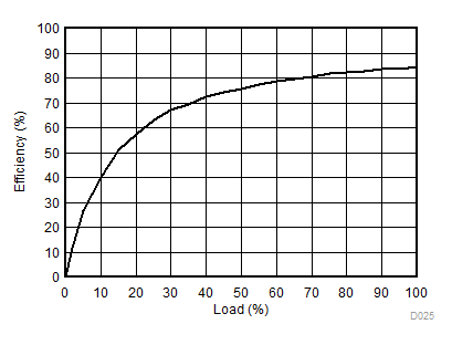
DCPA10505 DCPA10505D DCPA10512 DCPA10512D DCPA10515 DCPA10515D 12Veff.gif
DCPA10512
Figure 5. Efficiency vs Load
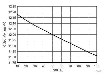
DCPA10505 DCPA10505D DCPA10512 DCPA10512D DCPA10515 DCPA10515D 12VLoadReg.gif
DCPA10512
Figure 7. Load Regulation
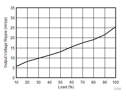
DCPA10505 DCPA10505D DCPA10512 DCPA10512D DCPA10515 DCPA10515D 12Vripple2.gif
DCPA10512 COUT = 1 µF
20-MHz BW
Figure 6. Output Ripple vs Load
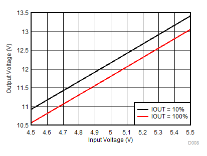
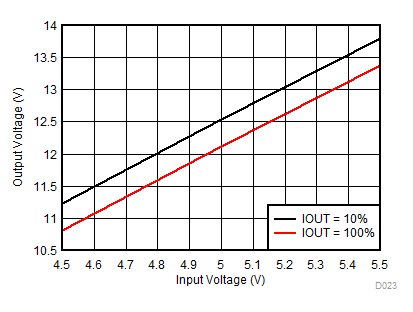
DCPA10505 DCPA10505D DCPA10512 DCPA10512D DCPA10515 DCPA10515D 12VlineReg2.gif
DCPA10512
Figure 8. Line Regulation

Typical Characteristics (DCPA10515)

At TA = 25°C, +VS = nominal, (unless otherwise noted)
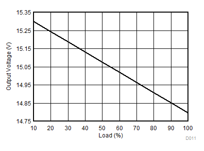
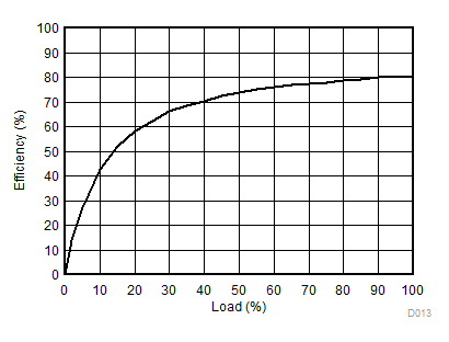
DCPA10505 DCPA10505D DCPA10512 DCPA10512D DCPA10515 DCPA10515D 15Veff.gif
DCPA10515
Figure 9. Efficiency vs Load
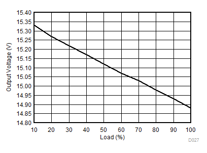
DCPA10505 DCPA10505D DCPA10512 DCPA10512D DCPA10515 DCPA10515D 15Vloadreg2.gif
DCPA10515
Figure 11. Load Regulation
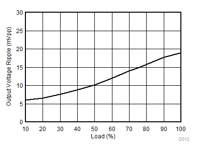
DCPA10505 DCPA10505D DCPA10512 DCPA10512D DCPA10515 DCPA10515D 15Vripple2.gif
DCPA10515 COUT = 1 µF
20-MHz BW
Figure 10. Output Ripple vs Load
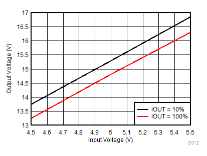
DCPA10505 DCPA10505D DCPA10512 DCPA10512D DCPA10515 DCPA10515D 15Vlinereg.gif
DCPA10515
Figure 12. Line Regulation

Typical Characteristics (DCPA10505D)

At TA = 25°C, +VS = nominal, (unless otherwise noted)
DCPA10505 DCPA10505D DCPA10512 DCPA10512D DCPA10515 DCPA10515D 5VDualEff.gif
DCPA10505D
Figure 13. Efficiency vs Load
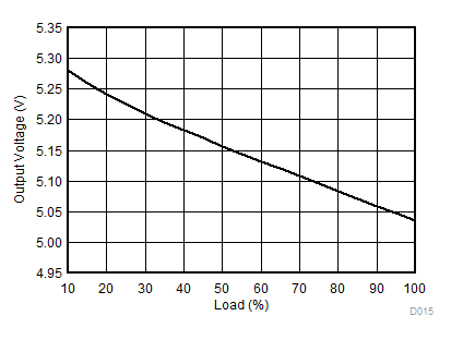
DCPA10505 DCPA10505D DCPA10512 DCPA10512D DCPA10515 DCPA10515D 5VDualposLoadReg.gif
DCPA10505D +VOUT
Figure 15. +VOUT Load Regulation
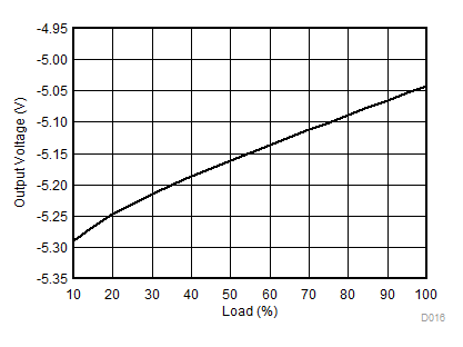
DCPA10505 DCPA10505D DCPA10512 DCPA10512D DCPA10515 DCPA10515D 5VDualnegLoadReg2.gif
DCPA10505D –VOUT
Figure 17. –VOUT Load Regulation
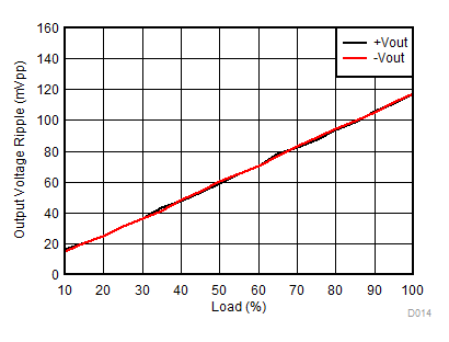
DCPA10505 DCPA10505D DCPA10512 DCPA10512D DCPA10515 DCPA10515D 5VDualripple2.gif
DCPA10505D COUT = 1 µF
20-MHz BW
Figure 14. Output Ripple vs Load
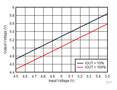
DCPA10505 DCPA10505D DCPA10512 DCPA10512D DCPA10515 DCPA10515D 5VDualposLineReg2.gif
DCPA10505D +VOUT
Figure 16. +VOUT Line Regulation
DCPA10505 DCPA10505D DCPA10512 DCPA10512D DCPA10515 DCPA10515D 5VDualnegLineReg2.gif
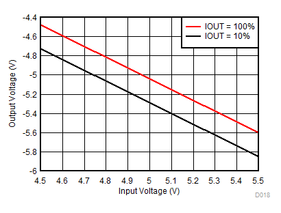
DCPA10505D –VOUT
Figure 18. –VOUT Line Regulation

Typical Characteristics (DCPA10512D)

At TA = 25°C, +VS = nominal, (unless otherwise noted)
DCPA10505 DCPA10505D DCPA10512 DCPA10512D DCPA10515 DCPA10515D 12VDualEff.gif
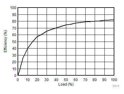
DCPA10512D
Figure 19. Efficiency vs Load
DCPA10505 DCPA10505D DCPA10512 DCPA10512D DCPA10515 DCPA10515D 12VDualposLoadreg.gif
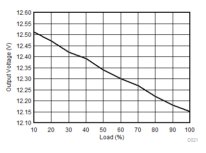
DCPA10512D +VOUT
Figure 21. +VOUT Load Regulation
DCPA10505 DCPA10505D DCPA10512 DCPA10512D DCPA10515 DCPA10515D 12VDualnegLoadreg.gif
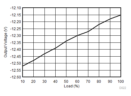
DCPA10512D –VOUT
Figure 23. –VOUT Load Regulation
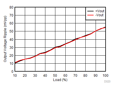
DCPA10505 DCPA10505D DCPA10512 DCPA10512D DCPA10515 DCPA10515D 12VDualripple2.gif
DCPA10512D COUT = 1 µF
20-MHz BW
Figure 20. Output Ripple vs Load
DCPA10505 DCPA10505D DCPA10512 DCPA10512D DCPA10515 DCPA10515D 12VDualposLinereg.gif
DCPA10512D +VOUT
Figure 22. +VOUT Line Regulation
DCPA10505 DCPA10505D DCPA10512 DCPA10512D DCPA10515 DCPA10515D 12VDualnegLinereg.gif
DCPA10512D –VOUT
Figure 24. –VOUT Line Regulation

Typical Characteristics (DCPA10515D)

At TA = 25°C, +VS = nominal, (unless otherwise noted)
DCPA10505 DCPA10505D DCPA10512 DCPA10512D DCPA10515 DCPA10515D 15VDualEff.gif
DCPA10515D
Figure 25. Efficiency vs Load
DCPA10505 DCPA10505D DCPA10512 DCPA10512D DCPA10515 DCPA10515D 15VDualposLoadreg.gif
DCPA10515D +VOUT
Figure 27. +VOUT Load Regulation
DCPA10505 DCPA10505D DCPA10512 DCPA10512D DCPA10515 DCPA10515D 15VDualnegLoadreg.gif
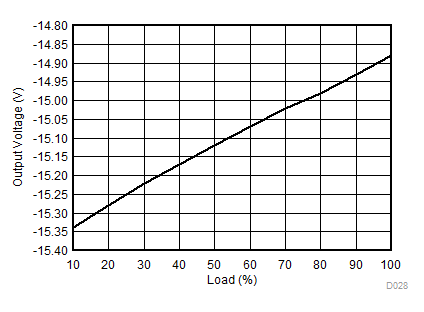
DCPA10515D –VOUT
Figure 29. –VOUT Load Regulation
DCPA10505 DCPA10505D DCPA10512 DCPA10512D DCPA10515 DCPA10515D 15VDualripple2.gif
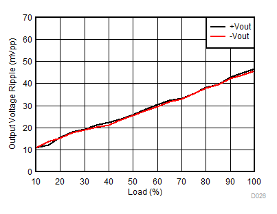
DCPA10515D COUT = 1 µF
20-MHz BW
Figure 26. Output Ripple vs Load
DCPA10505 DCPA10505D DCPA10512 DCPA10512D DCPA10515 DCPA10515D 15VDualposLinereg.gif
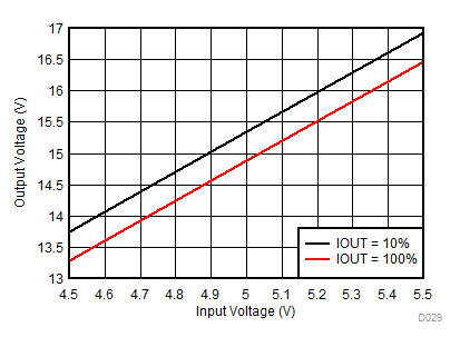
DCPA10515D +VOUT
Figure 28. +VOUT Line Regulation
DCPA10505 DCPA10505D DCPA10512 DCPA10512D DCPA10515 DCPA10515D 15VDualnegLinereg2.gif
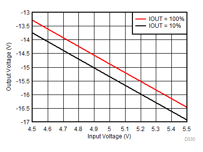
DCPA10515D –VOUT
Figure 30. –VOUT Line Regulation