DLPS119B December 2018 – May 2022 DLP2010NIR
PRODUCTION DATA
- 1 Features
- 2 Applications
- 3 Description
- 4 Revision History
- 5 Pin Configuration and Functions
-
6 Specifications
- 6.1 Absolute Maximum Ratings
- 6.2 Storage Conditions
- 6.3 ESD Ratings
- 6.4 Recommended Operating Conditions
- 6.5 Thermal Information
- 6.6 Electrical Characteristics
- 6.7 Timing Requirements
- 6.8 Switching Characteristics
- 6.9 System Mounting Interface Loads
- 6.10 Physical Characteristics of the Micromirror Array
- 6.11 Micromirror Array Optical Characteristics
- 6.12 Window Characteristics
- 6.13 Chipset Component Usage Specification
- 6.14 Typical Characteristics
- 7 Detailed Description
- 8 Application and Implementation
- 9 Power Supply Recommendations
- 10Layout
- 11Device and Documentation Support
- 12Mechanical, Packaging, and Orderable Information
7.6 Micromirror Array Temperature Calculation
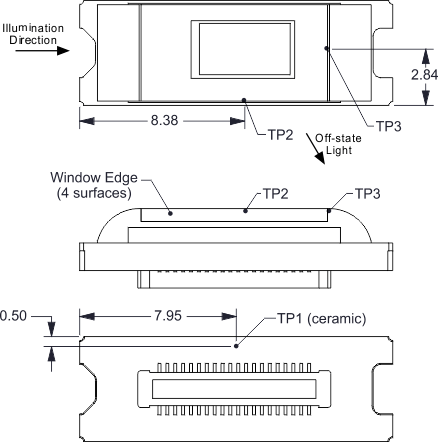
 Figure 7-1 DMD Thermal Test Points
Micromirror array temperature can be computed analytically from measurement points on the outside of the package, the ceramic package thermal resistance, the electrical power dissipation, and the illumination heat load. The relationship between micromirror array temperature and the reference ceramic temperature is provided by the following equations:
where
- TARRAY = Computed DMD array temperature (°C)
- TCERAMIC = Measured ceramic temperature (°C), TP1 location in Figure 7-1
- RARRAY–TO–CERAMIC = DMD package thermal resistance from array to outside ceramic (°C/W) specified in Section 6.5
- QARRAY = Total DMD power; electrical, specified in Electrical Characteristics, plus absorbed (calculated) (W)
- QELECTRICAL = Nominal DMD electrical power dissipation (W), specified in Electrical Characteristics
- AILLUMINATION = Illumination area (assumes 83.7% on the active array and 16.3% overfill)
- PNIR = Illumination Power Density (W/cm2)
Electrical power dissipation of the DMD is variable and depends on the voltages, data rates and operating frequencies. Refer to the specifications in Electrical Characteristics. Absorbed power from the illumination source is variable and depends on the operating state of the mirrors and the intensity of the light source. The DMD absorption constant of 0.42 assumes nominal operation with an illumination distribution of 83.7% on the DMD active array, and 16.3% on the DMD array border and window aperture.
A sample calculation is detailed below:
| TCERAMIC = 35 °C, assumed system measurement; see Recommended Operating Conditions for specification limits | |
| PNIR= 2 W/cm2 | |
| QELECTRICAL = 0.0908 W; See the table notes in Recommended Operating Conditions for details. | |
| AILLUMINATION = 0.143 cm2 | |
| QARRAY = QELECTRICAL + (QILLUMINATION X DMD absoprtion factor) = 0.0908 W + (2 W/cm2 X 0.143 cm2 X 0.42) = 0.211 W | |
| TARRAY = 35 °C + (0.211 W × 7.9°C/W) = 36.67 °C |