DLPS036B September 2014 – October 2016 DLP9000
PRODUCTION DATA.
- 1 Features
- 2 Applications
- 3 Description
- 4 Revision History
- 5 Description (continued)
- 6 Pin Configuration and Functions
-
7 Specifications
- 7.1 Absolute Maximum Ratings
- 7.2 Storage Conditions
- 7.3 ESD Ratings
- 7.4 Recommended Operating Conditions
- 7.5 Thermal Information
- 7.6 Electrical Characteristics
- 7.7 Timing Requirements
- 7.8 Capacitance at Recommended Operating Conditions
- 7.9 Typical Characteristics
- 7.10 System Mounting Interface Loads
- 7.11 Micromirror Array Physical Characteristics
- 7.12 Micromirror Array Optical Characteristics
- 7.13 Optical and System Image Quality
- 7.14 Window Characteristics
- 7.15 Chipset Component Usage Specification
- 8 Parameter Measurement Information
- 9 Detailed Description
- 10Application and Implementation
- 11Power Supply Requirements
- 12Layout
- 13Device and Documentation Support
- 14Mechanical, Packaging, and Orderable Information
7 Specifications
7.1 Absolute Maximum Ratings
over operating free-air temperature range (unless otherwise noted) (1)| MIN | MAX | UNIT | |||
|---|---|---|---|---|---|
| SUPPLY VOLTAGES | |||||
| VCC | Supply voltage for LVCMOS core logic (2) | –0.5 | 4 | V | |
| VCCI | Supply voltage for LVDS receivers (2) | –0.5 | 4 | V | |
| VOFFSET | Supply voltage for HVCMOS and micromirror electrode (2) (3) | –0.5 | 9 | V | |
| VBIAS | Supply voltage for micromirror electrode (2) | –0.5 | 17 | V | |
| VRESET | Supply voltage for micromirror electrode (2) | –11 | 0.5 | V | |
| | VCC – VCCI | | Supply voltage delta (absolute value) (4) | 0.3 | V | ||
| | VBIAS – VOFFSET | | Supply voltage delta (absolute value) (5) | 8.75 | V | ||
| INPUT VOLTAGES | |||||
| Input voltage for all other LVCMOS input pins (2) | –0.5 | VCC + 0.3 | V | ||
| Input voltage for all other LVDS input pins (2) (6) | –0.5 | VCCI + 0.3 | V | ||
| | VID | | Input differential voltage (absolute value) (7) | 700 | mV | ||
| IID | Input differential current (7) | 7 | mA | ||
| CLOCKS | |||||
| ƒclock | DLP9000 | Clock frequency for LVDS interface, DCLK_A | 440 | MHz | |
| Clock frequency for LVDS interface, DCLK_B | 440 | ||||
| Clock frequency for LVDS interface, DCLK_C | 440 | ||||
| Clock frequency for LVDS interface, DCLK_D | 440 | ||||
| DLP9000X | Clock frequency for LVDS interface, DCLK_A | 500 | |||
| Clock frequency for LVDS interface, DCLK_B | 500 | ||||
| Clock frequency for LVDS interface, DCLK_C | 500 | ||||
| Clock frequency for LVDS interface, DCLK_D | 500 | ||||
| ENVIRONMENTAL | |||||
| TARRAY | Array temperature: operational (8) (9) | 0 | 90 | ºC | |
| Array temperature: non–operational (9) | -40 | 90 | |||
| TWINDOW | Window temperature: operational | 0 | 70 | ºC | |
| Window temperature: non–operational | -40 | 90 | |||
| |TDELTA| | Absolute termperature delta between the window test points and the ceramic test point TP1(10) | 10 | ºC | ||
| RH | Relative Humidity, operating and non–operating | 95% | |||
7.2 Storage Conditions
applicable before the DMD is installed in the final product| MIN | MAX | UNIT | |||
|---|---|---|---|---|---|
| TDMD | DMD storage temperature | -40 | 80 | °C | |
| RH | Relative Humidity, (non-condensing) | 95% | |||
7.3 ESD Ratings
| VALUE | UNIT | |||
|---|---|---|---|---|
| V(ESD) | Electrostatic discharge | Human body model (HBM), per ANSI/ESDA/JEDEC JS-001, all pins (1) | ±2000 | V |
7.4 Recommended Operating Conditions
over operating free-air temperature range (unless otherwise noted)| MIN | NOM | MAX | UNIT | |||
|---|---|---|---|---|---|---|
| SUPPLY VOLTAGES (1) (2) | ||||||
| VCC | DLP9000 | Supply voltage for LVCMOS core logic | 3.0 | 3.3 | 3.6 | V |
| DLP9000X | Supply voltage for LVCMOS core logic | 3.3 | 3.45 | 3.6 | ||
| VCCI | DLP9000 | Supply voltage for LVDS receivers | 3.0 | 3.3 | 3.6 | V |
| DLP9000X | Supply voltage for LVDS receivers | 3.3 | 3.45 | 3.6 | ||
| VOFFSET | Supply voltage for HVCMOS and micromirror electrodes (3) | 8.25 | 8.5 | 8.75 | V | |
| VBIAS | Supply voltage for micromirror electrodes | 15.5 | 16 | 16.5 | V | |
| VRESET | –9.5 | –10 | –10.5 | V | ||
| |VCCI–VCC| | Supply voltage delta (absolute value) (4) | 0.3 | V | |||
| |VBIAS–VOFFSET| | Supply voltage delta (absolute value) (5) | 8.75 | V | |||
| LVCMOS PINS | ||||||
| VIH | High level Input voltage (6) | 1.7 | 2.5 | VCC + 0.3 | V | |
| VIL | Low level Input voltage (6) | – 0.3 | 0.7 | V | ||
| IOH | High level output current at VOH = 2.4 V | –20 | mA | |||
| IOL | Low level output current at VOL = 0.4 V | 15 | mA | |||
| TPWRDNZ | PWRDNZ pulse width (7) | 10 | ns | |||
| SCP INTERFACE | ||||||
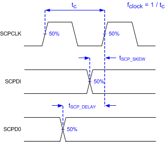
| ƒclock | SCP clock frequency (8) | 500 | kHz | |||
| tSCP_SKEW | Time between valid SCPDI and rising edge of SCPCLK (17) | –800 | 800 | ns | ||
| tSCP_DELAY | Time between valid SCPDO and rising edge of SCPCLK (17) | 700 | ns | |||
| tSCP_BYTE_INTERVAL | Time between consecutive bytes | 1 | µs | |||
| tSCP_NEG_ENZ | Time between falling edge of SCPENZ and the first rising edge of SCPCLK | 30 | ns | |||
| tSCP_PW_ENZ | SCPENZ inactive pulse width (high level) | 1 | µs | |||
| tSCP_OUT_EN | Time required for SCP output buffer to recover after SCPENZ (from tri-state) | 1.5 | ns | |||
| ƒclock | SCP circuit clock oscillator frequency (9) | 9.6 | 11.1 | MHz | ||
| LVDS INTERFACE | ||||||
| ƒclock | DLP9000 | Clock frequency DCLK | 400 | MHz | ||
| DLP9000X | Clock frequency DCLK (10) | 400 | 480 | |||
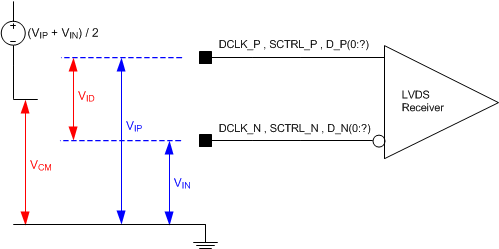
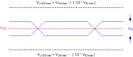
| |VID| | Input differential voltage (absolute value) (18) | 100 | 400 | 600 | mV | |
| VCM | Common mode (18) | 1200 | mV | |||
| VLVDS | LVDS voltage (18) | 0 | 2000 | mV | ||
| tLVDS_RSTZ | Time required for LVDS receivers to recover from PWRDNZ | 10 | ns | |||
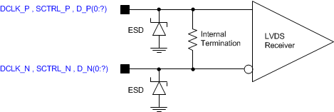
| ZIN | Internal differential termination resistance | 95 | 105 | Ω | ||
| ZLINE | Line differential impedance (PWB/trace) | 90 | 100 | 110 | Ω | |
| ENVIRONMENTAL (11) For Illumination Source Between 420 nm and 700 nm | ||||||
| TARRAY | DLP9000 | Array temperature, Long–term operational (13) (12)(19) | 10 | 40 to 65 (14) | °C | |
| Array temperature, Short–term operational (13) (12)(20) | 0 | 10 | ||||
| DLP9000X | Array temperature, Long–term operational (13) (12)(19) | 10 | 40 (21) | |||
| Array temperature, Short–term operational (13) (12)(20) | 0 | 10 | ||||
| TWINDOW | DLP9000 | Window Temperature test points TP2 and TP3, Long-term operational(19) | 10 | 70 | °C | |
| DLP9000X | Window Temperature test points TP2 and TP3, Long-term operational(19) | 10 | 40 | |||
| |TDELTA| | Absolute Temperature delta between the window test points (TP2, TP3) and the ceramic test point TP1(15) | 10 | °C | |||
| ILLVIS | Illumination | Thermally Limited (16) | mW/cm2 | |||
| RH | Relative Humidity (non-condensing) | 95% | ||||
| ENVIRONMENTAL (11) For Illumination Source Between 400 nm and 420 nm | ||||||
| TARRAY | Array temperature, Long–term operational (13) (12)(19) | 20 | 30 | °C | ||
| Array temperature, Short–term operational (13) (12)(20) | 0 | 20 | ||||
| TWINDOW | Window Temperature test points TP2 and TP3, Long-term operational(19) | 30 | °C | |||
| |TDELTA| | Absolute Temperature delta between the window test points (TP2, TP3) and the ceramic test point TP1(15) | 10 | °C | |||
| ILLVIS | Illumination | 10 | W/cm2 | |||
| RH | Relative Humidity (non-condensing) | 95% | ||||
| ENVIRONMENTAL (11) For Illumination Source <400 nm and >700 nm | ||||||
| TARRAY | DLP9000 | Array temperature, Long–term operational (13) (12)(19) | 10 | 40 to 65 (14) | °C | |
| Array temperature, Short–term operational (13) (12)(20) | 0 | 10 | ||||
| DLP9000X | Array temperature, Long–term operational (13) (12)(19) | 10 | 40 (21) | |||
| Array temperature, Short–term operational (13) (12)(20) | 0 | 10 | ||||
| TWINDOW | DLP9000 | Window Temperature test points TP2 and TP3, Long-term operational(19) | 10 | 70 | °C | |
| DLP9000X | Window Temperature test points TP2 and TP3, Long-term operational(19) | 10 | 40 | |||
| |TDELTA| | Absolute Temperature delta between the window test points (TP2, TP3) and the ceramic test point TP1(15) | 10 | °C | |||
| ILLUV | Illumination, wavelength < 400 nm | 0.68 | mW/cm2 | |||
| ILLIR | Illumination, wavelength > 700 nm | 10 | mW/cm2 | |||
| RH | Relative Humidity (non-condensing) | 95% | ||||
Frequency = 60 MHz. Maximum Rise Time = 2.5 ns at (20% to 80%)
Frequency = 60 MHz. Maximum Fall Time = 2.5 ns at (80% to 20%)
7.5 Thermal Information
| THERMAL METRIC (1) | DLP9000 | UNIT | ||
|---|---|---|---|---|
| FLS (CLGA) | ||||
| 355 PINS | ||||
| RθJA | Thermal resistance, active area to test point 1 (TP1) (max) | 0.5 | °C/W | |
7.6 Electrical Characteristics
over operating free-air temperature range (unless otherwise noted)| PARAMETER | TEST CONDITIONS (1) | MIN | TYP | MAX | UNIT | |
|---|---|---|---|---|---|---|
| VOH | High-level output voltage | VCC = 3 V, IOH = –20 mA | 2.4 | V | ||
| VOL | Low level output voltage | VCC = 3.6, IOL = 15 mA | 0.4 | V | ||
| IIH | High–level input current (2) (3) | VCC = 3.6 V, VI = VCC | 250 | µA | ||
| IlL | Low level input current | VCC = 3.6 V, VI = 0 | –250 | µA | ||
| IOZ | High–impedance output current | VCC = 3.6 V | 10 | µA | ||
| CURRENT | ||||||
| ICC | Supply current (4) | DLP9000 VCC = 3.6 V, DCLK=400 MHz | 1600 | mA | ||
| DLP9000X VCC = 3.6V, DCLK=480 MHz | 1850 | |||||
| ICCI | DLP9000 VCCI = 3.6 V, DCLK=400 MHz | 985 | ||||
| DLP9000X VCCI = 3.6, DCLK=480 MHz | 1100 | |||||
| IOFFSET | Supply current (5) | VOFFSET = 8.75 V | 25 | mA | ||
| IBIAS | VBIAS = 16.5 V | 14 | ||||
| IRESET | Supply current | VRESET = –10.5 V | 11 | mA | ||
| ITOTAL | DLP9000 Total Sum | 2634 | ||||
| DLP9000X Total Sum | 3000 | |||||
| POWER | ||||||
| PCC | Supply power dissipation | DLP9000 VCC = 3.6 V | 5760 | mW | ||
| DLP9000X VCC = 3.6 V | 6660 | |||||
| PCCI | DLP9000 VCCI = 3.6 V | 3546 | mW | |||
| DLP9000X VCCI = 3.6 V | 3960 | |||||
| POFFSET | VOFFSET = 8.75 V | 219 | mW | |||
| PBIAS | VBIAS = 16.5 V | 231 | mW | |||
| PRESET | VRESET = –10.5 V | 115 | mW | |||
| PTOTAL | Supply power dissipation (6) | DLP9000 Total Sum, DCLK = 400 MHz | 9871 | mW | ||
| DLP9000X Total Sum, DCLK = 480 MHz | 11185 | |||||
| CAPACITANCE | ||||||
| CI | Input capacitance | ƒ = 1 MHz | 10 | pF | ||
| CO | Output capacitance | ƒ = 1 MHz | 10 | pF | ||
| Reset group capacitance MBRST(31:0) | ƒ = 1 MHz; 2560 × 50 micromirrors | 230 | 290 | pF | ||
7.7 Timing Requirements
over Recommended Operating Conditions (unless otherwise noted) (1)| MIN | NOM | MAX | UNIT | ||||
|---|---|---|---|---|---|---|---|
| SCP INTERFACE (2) | |||||||
| tr | Rise time | 20% to 80% | 200 | ns | |||
| tƒ | Fall time | 80% to 20% | 200 | ns | |||
| LVDS INTERFACE (2) | |||||||
| tr | Rise time | 20% to 80% | 100 | 400 | ps | ||
| tƒ | Fall time | 80% to 20% | 100 | 400 | ps | ||
| LVDS CLOCKS (3) | |||||||
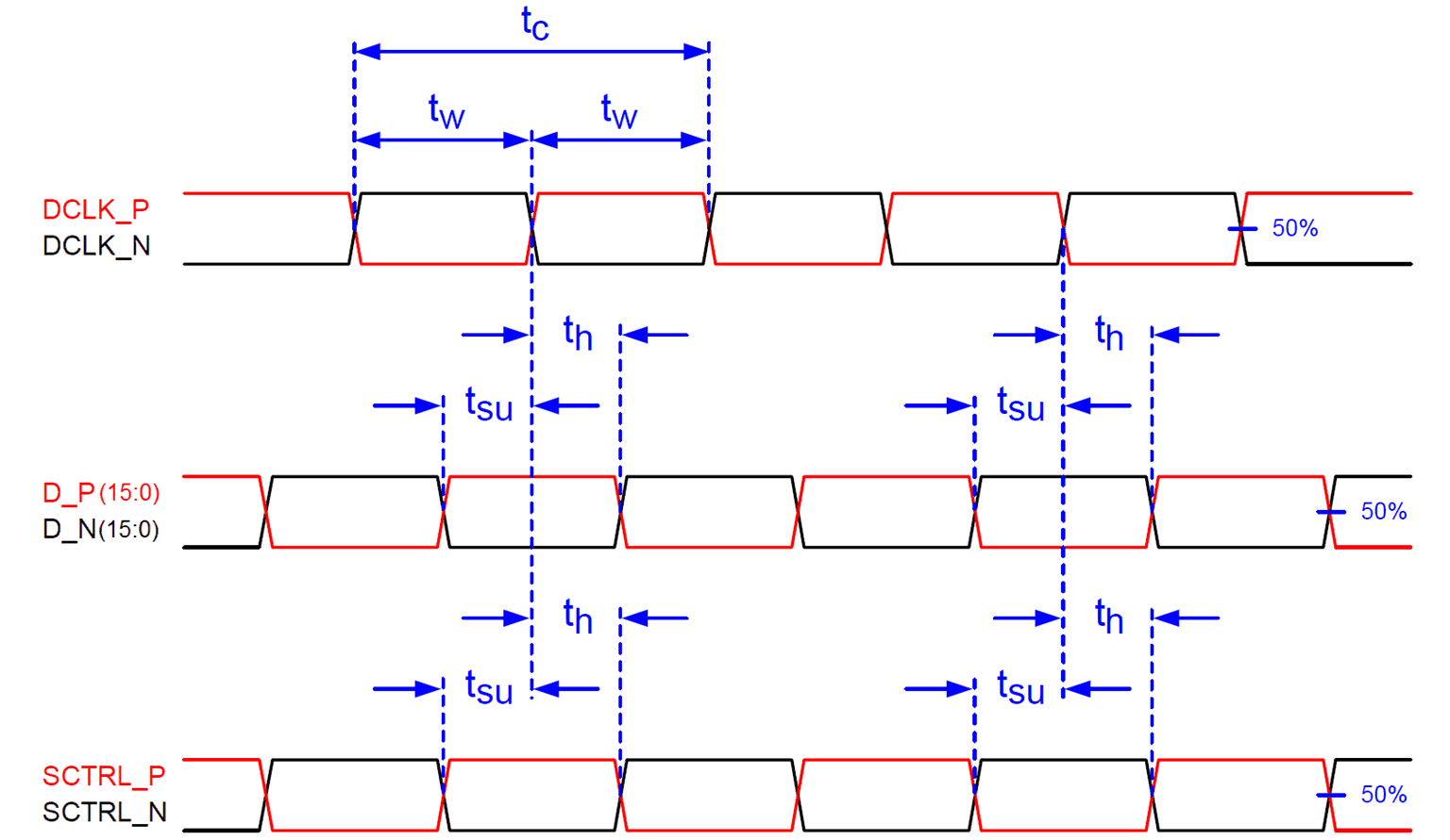
| tc | Cycle time | DLP9000 | DCLK_A, 50% to 50% | 2.5 | ns | ||
| DCLK_B, 50% to 50% | 2.5 | ||||||
| DCLK_C, 50% to 50% | 2.5 | ||||||
| DCLK_D, 50% to 50% | 2.5 | ||||||
| DLP9000X | DCLK_A, 50% to 50% | 2.083 | |||||
| DCLK_B, 50% to 50% | 2.083 | ||||||
| DCLK_C, 50% to 50% | 2.083 | ||||||
| DCLK_D, 50% to 50% | 2.083 | ||||||
| tw | Pulse duration | DLP9000 | DCLK_A, 50% to 50% | 1.19 | 1.25 | ns | |
| DCLK_B, 50% to 50% | 1.19 | 1.25 | |||||
| DCLK_C, 50% to 50% | 1.19 | 1.25 | |||||
| DCLK_D, 50% to 50% | 1.19 | 1.25 | |||||
| DLP9000X | DCLK_A, 50% to 50% | 1.031 | 1.042 | ||||
| DCLK_B, 50% to 50% | 1.031 | 1.042 | |||||
| DCLK_C, 50% to 50% | 1.031 | 1.042 | |||||
| DCLK_D, 50% to 50% | 1.031 | 1.042 | |||||
| LVDS INTERFACE (3) | |||||||
| tsu | Setup time | D_A(15:0) before rising or falling edge of DCLK_A | 0.2 | ns | |||
| D_B(15:0) before rising or falling edge of DCLK_B | 0.2 | ||||||
| D_C(15:0) before rising or falling edge of DCLK_C | 0.2 | ||||||
| D_D(15:0) before rising or falling edge of DCLK_D | 0.2 | ||||||
| tsu | Setup time | SCTRL_A before rising or falling edge of DCLK_A | 0.2 | ns | |||
| SCTRL_B before rising or falling edge of DCLK_B | 0.2 | ||||||
| SCTRL_C before rising or falling edge of DCLK_C | 0.2 | ||||||
| SCTRL_D before rising or falling edge of DCLK_D | 0.2 | ||||||
| th | Hold time | DLP9000 | D_A(15:0) after rising or falling edge of DCLK_A | 0.5 | ns | ||
| D_B(15:0) after rising or falling edge of DCLK_B | 0.5 | ||||||
| D_C(15:0) after rising or falling edge of DCLK_C | 0.5 | ||||||
| D_D(15:0) after rising or falling edge of DCLK_D | 0.5 | ||||||
| DLP9000X | D_A(15:0) after rising or falling edge of DCLK_A | 0.4 | |||||
| D_B(15:0) after rising or falling edge of DCLK_B | 0.4 | ||||||
| D_C(15:0) after rising or falling edge of DCLK_C | 0.4 | ||||||
| D_D(15:0) after rising or falling edge of DCLK_D | 0.4 | ||||||
| th | Hold time | DLP9000 | SCTRL_A after rising or falling edge of DCLK_A | 0.5 | ns | ||
| SCTRL_B after rising or falling edge of DCLK_B | 0.5 | ||||||
| SCTRL_C after rising or falling edge of DCLK_C | 0.5 | ||||||
| SCTRL_D after rising or falling edge of DCLK_D | 0.5 | ||||||
| DLP9000X | SCTRL_A after rising or falling edge of DCLK_A | 0.4 | |||||
| SCTRL_B after rising or falling edge of DCLK_B | 0.4 | ||||||
| SCTRL_C after rising or falling edge of DCLK_C | 0.4 | ||||||
| SCTRL_D after rising or falling edge of DCLK_D | 0.4 | ||||||
| LVDS INTERFACE (3) | |||||||
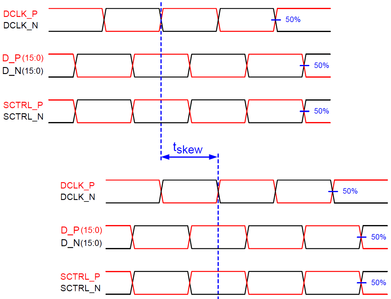
| tskew | Skew time | Channel B relative to Channel A | DLP9000 Channel A includes the following LVDS pairs: DCLK_AP and DCLK_AN SCTRL_AP and SCTRL_AN D_AP(15:0) and D_AN(15:0) |
–1.25 | 1.25 | ns | |
| DLP9000 Channel B includes the following LVDS pairs: DCLK_BP and DCLK_BN SCTRL_BP and SCTRL_BN D_BP(15:0) and D_BN(15:0) |
|||||||
| DLP9000X Channel A includes the following LVDS pairs: DCLK_AP and DCLK_AN SCTRL_AP and SCTRL_AN D_AP(15:0) and D_AN(15:0) |
-1.04 | 1.04 | ns | ||||
| DLP9000X Channel B includes the following LVDS pairs: DCLK_BP and DCLK_BN SCTRL_BP and SCTRL_BN D_BP(15:0) and D_BN(15:0) |
|||||||
| Channel D relative to Channel C | DLP9000 Channel C includes the following LVDS pairs: DCLK_CP and DCLK_CN SCTRL_CP and SCTRL_CN D_CP(15:0) and D_CN(15:0) |
–1.25 | 1.25 | ns | |||
| DLP9000 Channel D includes the following LVDS pairs: DCLK_DP and DCLK_DN SCTRL_DP and SCTRL_DN D_DP(15:0) and D_DN(15:0) |
|||||||
| DLP9000X Channel C includes the following LVDS pairs: DCLK_CP and DCLK_CN SCTRL_CP and SCTRL_CN D_CP(15:0) and D_CN(15:0) |
-1.04 | 1.04 | ns | ||||
| DLP9000X Channel D includes the following LVDS pairs: DCLK_DP and DCLK_DN SCTRL_DP and SCTRL_DN D_DP(15:0) and D_DN(15:0) |
|||||||

7.8 Capacitance at Recommended Operating Conditions
over operating free-air temperature range (unless otherwise noted)| PARAMETER | TEST CONDITIONS | MIN | MAX | UNIT | |
|---|---|---|---|---|---|
| CI | Input capacitance | ƒ = 1 MHz | 10 | pF | |
| CO | Output capacitance | ƒ = 1 MHz | 10 | pF | |
| CIM | MBRST(31:0) input capacitance | f = 1 MHz. All inputs interconnected. | 230 | 290 | pF |
7.9 Typical Characteristics
When the DLP9000 DMD is controlled by two DLPC900 controllers, these digital controllers offer four modes of operation.
- Video Mode
- Video Pattern Mode
- Pre-Stored Pattern Mode
- Pattern On-The-Fly Mode
In video mode, the video source is displayed on the DMD at the rate of the incoming video source.
In modes 2, 3, and 4, the pattern rates depend on the bit depth as shown in Table 1.
When the DLP9000X DMD is controlled by the DLPC910 controller, the digital controller offers streaming 1-bit binary patterns to the DMD at speeds greater than 61 Gigabits per second (Gbps). The patterns are streamed from a customer designed applications processor into the DLPC910 input LVDS data interface. Table 2 shows the pattern rates for the different DMD Reset Modes.
Table 1. DLPC900 with DLP9000 Pattern Rate versus Bit Depth
| BIT DEPTH | VIDEO PATTERN MODE (Hz) | PRE-STORED or PATTERN ON-THE-FLY MODE (Hz) |
|---|---|---|
| 1 | 2880 | 9523 |
| 2 | 1440 | 3289 |
| 3 | 960 | 2638 |
| 4 | 720 | 1364 |
| 5 | 480 | 823 |
| 6 | 480 | 672 |
| 7 | 360 | 500 |
| 8 | 247 | 247 |
Table 2. DLPC910 with DLP9000X Pattern Rates versus Reset Mode
| RESET MODE(1) | MAX PIXEL DATA RATE (Gbps)(2) | MAX PATTERN RATE (Hz) (5) |
|---|---|---|
| Global | 53.42 | 13043(3) |
| Single | 56.46 | 13783 (4) |
| Dual | 59.89 | 14624 (4) |
| Quad | 61.39 | 14989(4) |
7.10 System Mounting Interface Loads
| PARAMETER | MIN | NOM | MAX | UNIT | ||
|---|---|---|---|---|---|---|
| Maximum system mounting interface load to be applied to the: | Thermal interface area (See Figure 8) | 35 | lbs | |||
| Electrical interface area | 300 | lbs | ||||
| Datum A interface area (1) | 160 | lbs | ||||
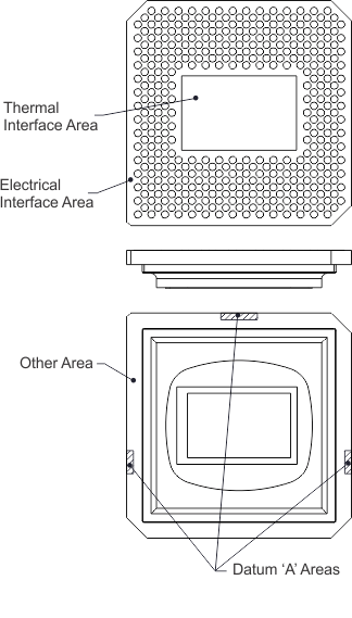 Figure 8. System Mounting Interface Loads
7.11 Micromirror Array Physical Characteristics
| VALUE | UNIT | ||||
|---|---|---|---|---|---|
| M | Number of active columns | See Figure 9 | 2560 | micromirrors | |
| N | Number of active rows | 1600 | micromirrors | ||
| P | Micromirror (pixel) pitch | 7.56 | µm | ||
| Micromirror active array width | M × P | 19.3536 | mm | ||
| Micromirror active array height | N × P | 12.096 | mm | ||
| Micromirror active border | Pond of micromirror (POM) (1) | 14 | micromirrors/ side | ||
| Micromirror total area | P2 x M x N (converted to cm) | 2.341 | cm2 | ||
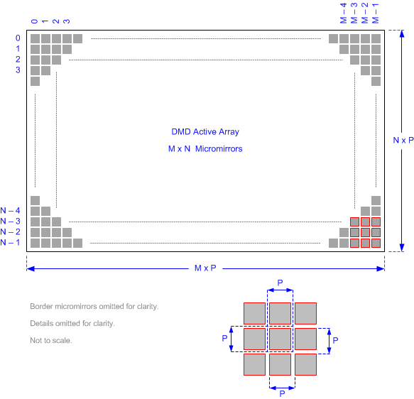
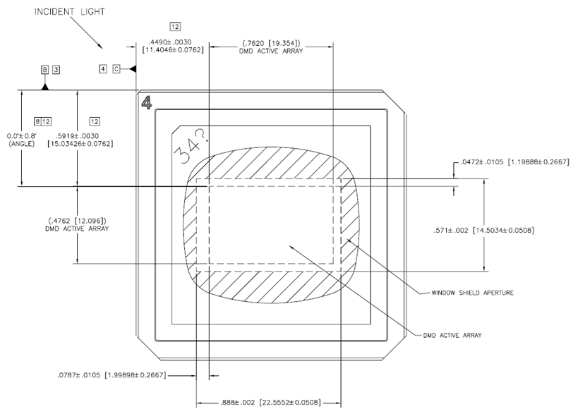 Figure 10. DMD Micromirror Active Area
7.12 Micromirror Array Optical Characteristics
Refer to Optical Interface and System Image Quality for important information.
| PARAMETER | TEST CONDITIONS | MIN | NOM | MAX | UNIT | |
|---|---|---|---|---|---|---|
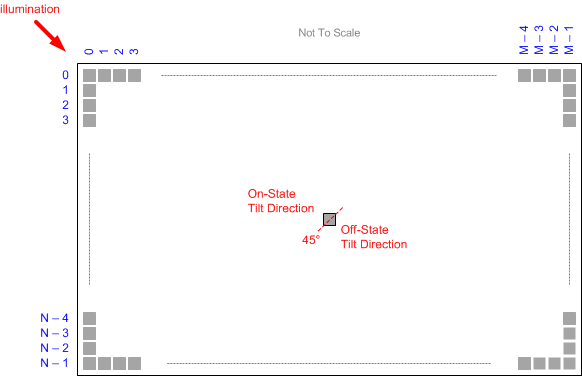
| α | Micromirror tilt angle | DMD landed state (1) | 12 | ° | ||
| β | Micromirror tilt angle tolerance (1) (2) (3) (4) (5) | –1 | 1 | ° | ||
| Micromirror tilt direction (5) (6) | See Figure 11 | 44 | 45 | 46 | ° | |
| Number of out-of-specification micromirrors (7) | Adjacent micromirrors | 0 | micromirrors | |||
| Non-adjacent micromirrors | 10 | |||||
| Micromirror crossover time (8) (9) | Typical performance | 2.5 | μs | |||
| DMD efficiency within the wavelength range 400 nm to 420 nm (10) | 68% | |||||
| DMD photopic efficiency within the wavelength range 420 nm to 700 nm (10) | 66% | |||||
7.13 Optical and System Image Quality
Optimizing system optical performance and image quality strongly relate to optical system design parameter trades. Although it is not possible to anticipate every conceivable application, projector image quality and optical performance is contingent on compliance to the optical system operating conditions described in a) through c) below:
- Numerical Aperture and Stray Light Control. The angle defined by the numerical aperture of the illumination and projection optics at the DMD optical area should be the same. This angle should not exceed the nominal device mirror tilt angle unless appropriate apertures are added in the illumination and/or projection pupils to block out flat-state and stray light from the projection lens. The mirror tilt angle defines DMD capability to separate the "ON" optical path from any other light path, including undesirable flat-state specular reflections from the DMD window, DMD border structures, or other system surfaces near the DMD such as prism or lens surfaces. If the numerical aperture exceeds the mirror tilt angle, or if the projection numerical aperture angle is more than two degrees larger than the illumination numerical aperture angle, objectionable artifacts in the display’s border and/or active area could occur.
- Pupil Match. TI’s optical and image quality specifications assume that the exit pupil of the illumination optics is nominally centered within two degrees of the entrance pupil of the projection optics. Misalignment of pupils can create objectionable artifacts in the display’s border and/or active area, which may require additional system apertures to control, especially if the numerical aperture of the system exceeds the pixel tilt angle.
- Illumination Overfill. Overfill light illuminating the area outside the active array can create artifacts from the mechanical features that surround the active array and other surface anomalies that may be visible on the screen. The illumination optical system should be designed to limit light flux incident anywhere outside the active array more than 20 pixels from the edge of the active array on all sides. Depending on the particular system’s optical architecture and assembly tolerances, this amount of overfill light on the outside of the active array may still cause artifacts to still be visible.
NOTE
TI ASSUMES NO RESPONSIBILITY FOR IMAGE QUALITY ARTIFACTS OR DMD FAILURES CAUSED BY OPTICAL SYSTEM OPERATING CONDITIONS EXCEEDING LIMITS DESCRIBED ABOVE.
7.14 Window Characteristics
| PARAMETER (1) | TEST CONDITIONS | MIN | TYP | MAX | UNIT |
|---|---|---|---|---|---|
| Window material designation | Corning 7056 | ||||
| Window refractive index | at wavelength 589 nm | 1.487 | |||
| Window aperture | See (2) | ||||
| Illumination overfill | Refer to Illumination Overfill | ||||
| Window transmittance, single–pass through both surfaces and glass (3) | At wavelength 405 nm. Applies to 0° and 24° AOI only. | 95% | |||
| Minimum within the wavelength range 420 nm to 680 nm. Applies to all angles 0° to 30° AOI. | 97% | ||||
| Average over the wavelength range 420 nm to 680 nm. Applies to all angles 30° to 45° AOI. | 97% |
7.15 Chipset Component Usage Specification
The DMD is a component of one or more DLP® chipsets. Reliable function and operation of the DMD requires that it be used in conjunction with the other components of the applicable DLP chipset, including those components that contain or implement TI DMD control technology. TI DMD control technology is the TI technology and devices for operating or controlling a DMD.