ZHCS244C January 2012 – August 2015 DLPC300
PRODUCTION DATA.
- 1 特性
- 2 应用
- 3 说明
- 4 修订历史记录
- 5 Pin Configuration and Functions
-
6 Specifications
- 6.1 Absolute Maximum Ratings
- 6.2 ESD Ratings
- 6.3 Recommended Operating Conditions
- 6.4 Thermal Information
- 6.5 I/O Electrical Characteristics
- 6.6 Crystal Port Electrical Characteristics
- 6.7 Power Consumption
- 6.8 I2C Interface Timing Requirements
- 6.9 Parallel Interface Frame Timing Requirements
- 6.10 Parallel Interface General Timing Requirements
- 6.11 Parallel I/F Maximum Supported Horizontal Line Rate
- 6.12 BT.565 I/F General Timing Requirements
- 6.13 Flash Interface Timing Requirements
- 6.14 DMD Interface Timing Requirements
- 6.15 Mobile Dual Data Rate (mDDR) Memory Interface Timing Requirements
- 6.16 JTAG Interface: I/O Boundary Scan Application Switching Characteristics
- 7 Detailed Description
-
8 Application and Implementation
- 8.1 Application Information
- 8.2 Typical Application
- 8.3 System Examples
- 9 Power Supply Recommendations
-
10Layout
- 10.1
Layout Guidelines
- 10.1.1 Printed Circuit Board Design Guidelines
- 10.1.2 Printed Circuit Board Layer Stackup Geometry
- 10.1.3 Signal Layers
- 10.1.4 Routing Constraints
- 10.1.5 Termination Requirements
- 10.1.6 PLL
- 10.1.7 General Handling Guidelines for Unused CMOS-Type Pins
- 10.1.8 Hot-Plug Usage
- 10.1.9 External Clock Input Crystal Oscillator
- 10.2 Layout Example
- 10.3 Thermal Considerations
- 10.1
Layout Guidelines
- 11器件和文档支持
- 12机械、封装和可订购信息
7 Detailed Description
7.1 Overview
In DLP-based solutions, image data is 100% digital from the DLPC300 input port to the image on the DMD. The image stays in digital form and is never converted into an analog signal. The DLPC300 processes the digital input image and converts the data into a format needed by the DLP3000. The DLP3000 then steers light by using binary pulse-width-modulation (PWM) for each pixel mirror. Refer to the DLP3000 data sheet (DLPS022) for further details.
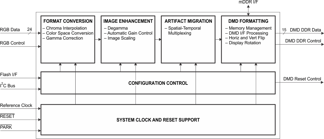
Figure 8 shows the DLPC300 functional block diagram. As part of the pixel processing functions, the DLPC300 offers format conversion functions: chroma interpolation for 4:2:2 and 4:4:4, color-space conversion, and gamma correction. The DLPC300 also offers several image-enhancement functions: programmable degamma, automatic gain control, and image resizing. Additionally, the DLPC300 offers an artifact migration function through spatial-temporal multiplexing (dithering). Finally, the DLPC300 offers the necessary functions to format the input data to the DMD. The pixel processing functions allow the DLPC300 and DLP3000 to support a wide variety of resolutions including NTSC, PAL, QVGA, QWVGA, VGA, and WVGA. The pixel processing functions can be optionally bypassed with the native 608 × 684 pixel resolution.
7.2 Functional Block Diagram
 Figure 8. DLPC300 Functional Block Diagram
7.3 Feature Description
When accurate pattern display is needed, the native 608 × 684 input resolution pattern has a one-to-one association with the corresponding micromirror on the DLP3000. The DLPC300 enables high-speed display of these patterns: up to 1440 Hz for binary (1-bit) patterns and up to 120 Hz for 8-bit patterns. This functionality is well-suited for techniques such as structured light, rapid manufacturing, or digital exposure.
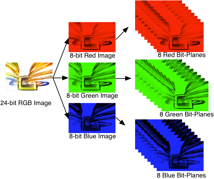
The DLPC300 takes as input 16-, 18-, or 24-bit RGB data at up to 60-Hz frame rate. This frame rate is composed of three colors (red, green, and blue) with each color equally divided in the 60-Hz frame rate. Thus, each color has a 5.55-ms time slot allocated. Because each color has 5-, 6-, or 8-bit depth, each color time slot is further divided into bit-planes. A bit-plane is the 2-D arrangement of one-bit extracted from all the pixels in the full color 2D image. See Figure 9.
 Figure 9. Bit Slices
The length of each bit-plane in the time slot is weighted by the corresponding power of 2 of its binary representation. This provides a binary pulse-width modulation of the image. For example, a 24-bit RGB input has three colors with 8-bit depth each. Each color time slot is divided into 8 bit-planes, with the sum of all bit planes in the time slot equal to 256. See Figure 10 for an illustration of this partition of the bits in a frame.
 Figure 10. Bit Partition in a Frame for an 8-Bit Color
Therefore, a single video frame is composed of a series of bit-planes. Because the DMD mirrors can be either on or off, an image is created by turning on the mirrors corresponding to the bit set in a bit-plane. With the binary pulse-width modulation, the intensity level of the color is reproduced by controlling the amount of time the mirror is on. For a 24-bit RGB frame, the DLPC300 creates 24 bit planes, stores them on the mDDR, and sends them to the DLP3000 DMD, one bit-plane at a time. Depending on the bit weight of the bit-plane, the DLPC300 controls the time this bit-plane is exposed to light, controlling the intensity of the bit-plane. To improve image quality in video frames, these bit-planes, time slots, and color frames are intertwined and interleaved with spatial-temporal algorithms by the DLPC300. In external video mode, the controller applies non-linear gamma correction.
7.4 Device Functional Modes
For applications where image enhancement is not desired, the video processing algorithms can be bypassed and replaced with a specific set of bit-planes. The bit-depth of the pattern is then allocated into the corresponding time slots. Furthermore, an output trigger signal is also synchronized with these time slots to indicate when the image is displayed. For structured light applications, this mechanism provides the capability to display a set of patterns and signal a camera to capture these patterns overlaid on an object. In this structured light mode, the controller applies linear gamma correction.
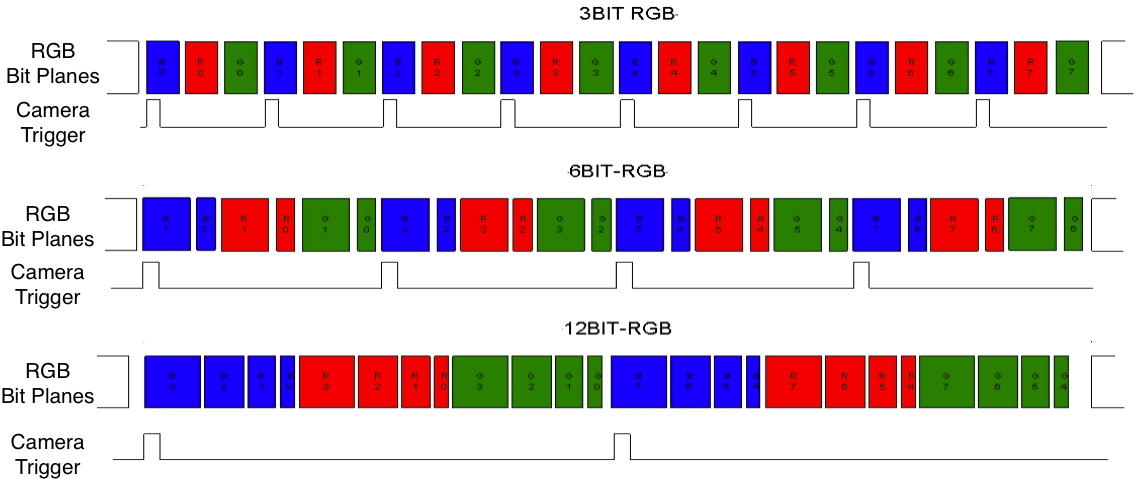
Figure 11 shows the bit planes and corresponding output triggers for 3-bit, 6-bit, and 12-bit RGB. Table 1 shows the allowed pattern combinations in relation to the bit depth of the pattern.
 Figure 11. Bit Planes and Output Trigger for 3-, 6-, and 12-Bit RGB Input
Table 1. Allowed Pattern Combinations
| External Video Sequence | Number of Images per Frame | Frame Rate | Pattern Rate | |
|---|---|---|---|---|
| Monochrome | 1 bit per pixel | 24 | 15, 30, 40, or 60 Hz | 24 × Frame rate |
| 2 bits per pixel | 12 | 12 × Frame rate | ||
| 3 bits per pixel | 8 | 15, 30, 45, or 60 Hz | 8 × Frame rate | |
| 4 bits per pixel | 6 | 15, 30, 40, or 60 Hz | 6 × Frame rate | |
| 5 bits per pixel | 4 | 15, 30, 45, or 60 Hz | 4 × Frame rate | |
| 6 bits per pixel | 4 | 4 × Frame rate | ||
| 7 bits per pixel | 3 | 15, 30, 40, or 60 Hz | 3 × Frame rate | |
| 8 bits per pixel | 2 | 15, 30, 45, or 60 Hz | 2 × Frame rate | |
| RGB | 1-bit per color pixel (3-bit per pixel) |
8 | 8 × Frame rate | |
| 2-bit per color pixel (6-bit per pixel) |
4 | 4 × Frame rate | ||
| 4-bit per color pixel (12-bit per pixel) |
2 | 2 × Frame rate | ||
| 5/6/5-bit RGB pixel (16-bit per pixel) |
1 | Frame rate | ||
| 6-bit per color pixel (18-bit per pixel) |
||||
| 8-bit per color pixel (24-bit per pixel) |
||||
7.4.1 Configuration Control
The primary configuration control mechanism for the DLPC300 is the I2C interface. See the DLPC300 Software Programmer's Guide (DLPU004) for details on how to configure and control the DLPC300.
7.4.2 Parallel Bus Interface
Parallel bus interface supports six data transfer formats:
- 16-bit RGB565
- 18-bit RGB666
- 18-bit 4:4:4 YCrCb666
- 24-bit RGB888
- 24-bit 4:4:4 YCrCb888
- 16-bit 4:2:2 YCrCb (standard sampling assumed to be Y0Cb0, Y1Cr0, Y2Cb2, Y3Cr2, Y4Cb4, Y5Cr4, …)
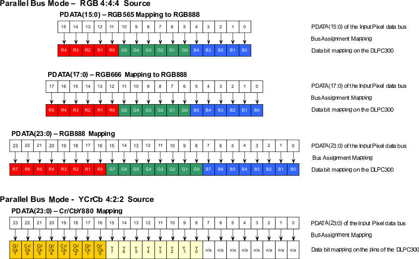
Figure 12 shows the required PDATA(23:0) bus mapping for these six data transfer formats.
 Figure 12. PDATA Bus – Parallel I/F Mode Bit Mapping
The parallel bus interface complies with the standard graphics interface protocol, which includes a vertical sync signal (VSYNC), horizontal sync signal (HSYNC), optional data-valid signal (DATAEN), a 24-bit data bus (PDATA), and a pixel clock (PCLK). The polarities of both syncs are programmable, as is the active edge of the clock. Figure 2 shows the relationship of these signals. The data-valid signal (DATAEN) is optional, in that the DLPC300 provides auto-framing parameters that can be programmed to define the data-valid window, based on pixel and line counting relative to the horizontal and vertical syncs.
7.4.3 BT.656 Interface
BT.656 data bits should be mapped to the DLPC300 PDATA bus as shown in Figure 13.
 Figure 13. PDATA Bus – BT.656 I/F Mode Bit Mapping