ZHCSE90D September 2015 – September 2020 DLPC910
PRODUCTION DATA
- 1 特性
- 2 应用
- 3 说明
- 4 Revision History
- 5 Pin Configuration and Functions
- 6 Specifications
-
7 Detailed Description
- 7.1 Overview
- 7.2 Functional Block Diagram
- 7.3 Feature Description
- 7.4 Device Functional Modes
- 7.5
Register Map
- 7.5.1
Register Table Overview
- 7.5.1.1 DESTOP_INTERRUPT Register
- 7.5.1.2 MAIN_STATUS Register
- 7.5.1.3 DESTOP_CAL Register
- 7.5.1.4 DESTOP_DMD_ID_REG Register
- 7.5.1.5 DESTOP_CATBITS_REG Register
- 7.5.1.6 DESTOP_VERSION Register
- 7.5.1.7 DESTOP_RESET_REG Register
- 7.5.1.8 DESTOP_INFIFO_STATUS Register
- 7.5.1.9 DESTOP_BUS_SWAP Register
- 7.5.1.10 DESTOP_DMDCTRL Register
- 7.5.1.11 DESTOP_BIT_FLIP Register
- 7.5.1
Register Table Overview
- 8 Application and Implementation
- 9 Power Supply Recommendations
- 10Layout
- 11Device and Documentation Support
- 12Mechanical, Packaging, and Orderable Information
7.4.4 Mirror Clocking Pulse
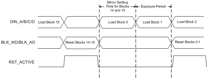
A Mirror Clocking Pulse (MCP) sequence begins by asserting BLKMD and BLKAD for a single, dual, quad, or global block operation as defined in Table 7-12. A MCP causes a reset on the block(s), and the data stored in the block(s) takes effect on the mirrors of the DMD. Shortly after a MCP has been issued, RST_ACTIVE goes high for approximately 4 μs, indicating a MCP operation is in progress. During this time, no additional MCPs may be initiated until RST_ACTIVE returns low. RST_ACTIVE does not return to low unless continuous no-op or data loading row cycles are issued. A typical single block load phased sequence in which consecutive DMD blocks are loaded is illustrated in Figure 7-8. A MCP time is identical for single, dual, quad or global block operations.
Note that it may take longer to complete a MCP on a block than it does to load a block. The block load time may be calculated as:
| DMD | MINIMUM BLOCK LOAD TIME | DCLKIN (MHz) |
|---|---|---|
| DLP9000X | 4.167 µsec | 480 |
| DLP9000XUV | 4.167 µsec | 480 |
| DLP6500 | 5.76 µsec | 400 |
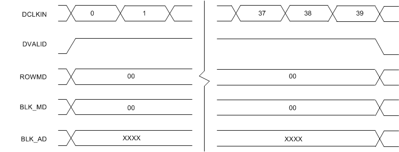
For any case which involves sending a MCP or a Block Clear without data loading, the customer interface must send no-op row cycles. This can be accomplished by asserting DVALID, while holding ROWMD at 00 and BLKMD at 00 for the number of clocks per row in the DMD, as in Figure 7-7. Refer to Table 7-11 to obtain the number of clocks per row. Following the loading of all rows in a block or the entire DMD, at least one no-op row cycle must be completed to initiate the MCP. If the MCP is asserted prior to loading all rows in a block or the entire DMD, rows which were not updated will show old data. Additional MCP operations may not be initiated until RST_ACTIVE is low. Block Clear operations for the DMD must be followed by two consecutive no-op row cycle commands.
To obtain full utilization of the DMD bandwidth, load four blocks and then issue a MCP to the four blocks concurrently by setting RST2BLKZ to 1 and BLKMD to 11 with the appropriate address in BLKAD. This is illustrated in Figure 7-10.
It is possible to load other blocks while the block(s) previously issued a MCP is settling. This is illustrated in Figure 7-9 and Figure 7-10, where blocks are reloaded while the mirror setting time is occurring. It is also possible to load other blocks while previously loaded block(s) have an outstanding RST_ACTIVE. This is illustrated in Figure 7-10, where block 0 is loaded while RST_ACTIVE is asserted for blocks 12-15.
While RST_ACTIVE is high for 4 μs, the data for the block(s) being issued a MCP should not be changed to allow the mirrors to become stable. The RST_ACTIVE does not include the mirror settling period. A short delay of 6 μs should be introduced during the last block(s) that is issued a MCP. The mirror settling time is illustrated in Figure 7-8, Figure 7-9, Figure 7-10, and Figure 7-11, where the customer interface introduces a delay on the last block(s) that were issued a MCP to allow the mirrors to become stable.
Figure 7-8, Figure 7-9, Figure 7-10, and Figure 7-11 all show an exposure period. Once the customer interface has issued all required MCPs and the proper mirror settling time has been applied, the customer interface may pulse an illumination source onto the DMD during this period. The exposure period is user adjustable; however, increasing the exposure period decreases the pattern rate. Refer to Application Curves regarding exposure period.
Figure 7-7, Figure 7-8, Figure 7-9, Figure 7-10, and Figure 7-11 show timing for the DLP9000X/DLP9000XUV. Refer to Table 7-11 to obtain the number of reset blocks and clocks per row for the DLP6500 DMD.
 Figure 7-7 DMD No-op Row Cycle
 Figure 7-8 Single Block Load Phased Sequence
 Figure 7-9 Dual Block Load Phased Sequence
 Figure 7-10 Quad Block Load Phased Sequence
 Figure 7-11 Full DMD Global Load Sequence
Note: After a MCP or Block Clear command is given, RST_ACTIVE may not be asserted until up to 60 ns (depending on the clock frequency) after the command. While RST_ACTIVE is asserted, no other command should be given.