ZHCSN76B January   2021  – April 2022 DRV8316

PRODUCTION DATA  

  1. 特性
  2. 应用
  3. 说明
  4. Revision History
  5. Device Comparison Table
  6. Pin Configuration and Functions
  7. Specifications
    1. 7.1 Absolute Maximum Ratings
    2. 7.2 ESD Ratings
    3. 7.3 Recommended Operating Conditions
    4. 7.4 Thermal Information
    5. 7.5 Electrical Characteristics
    6. 7.6 SPI Timing Requirements
    7. 7.7 SPI Slave Mode Timings
    8. 7.8 Typical Characteristics
  8. Detailed Description
    1. 8.1 Overview
    2. 8.2 Functional Block Diagram
    3. 8.3 Feature Description
      1. 8.3.1  Output Stage
      2. 8.3.2  Control Modes
        1. 8.3.2.1 6x PWM Mode (MODE = 00b or MODE Pin Tied to AGND)
        2. 8.3.2.2 3x PWM Mode (MODE = 10b or MODE Pin is Connected to AGND with RMODE)
        3. 8.3.2.3 Current Limit Mode (MODE = 01b / 11b or MODE Pin is Hi-Z or Connected to AVDD)
      3. 8.3.3  Device Interface Modes
        1. 8.3.3.1 Serial Peripheral Interface (SPI)
        2. 8.3.3.2 Hardware Interface
      4. 8.3.4  Step-Down Mixed-Mode Buck Regulator
        1. 8.3.4.1 Buck in Inductor Mode
        2. 8.3.4.2 Buck in Resistor mode
        3. 8.3.4.3 Buck Regulator with External LDO
        4. 8.3.4.4 AVDD Power Sequencing on Buck Regulator
        5. 8.3.4.5 Mixed mode Buck Operation and Control
      5. 8.3.5  AVDD Linear Voltage Regulator
      6. 8.3.6  Charge Pump
      7. 8.3.7  Slew Rate Control
      8. 8.3.8  Cross Conduction (Dead Time)
      9. 8.3.9  Propagation Delay
        1. 8.3.9.1 Driver Delay Compensation
      10. 8.3.10 Pin Diagrams
        1. 8.3.10.1 Logic Level Input Pin (Internal Pulldown)
        2. 8.3.10.2 Logic Level Input Pin (Internal Pullup)
        3. 8.3.10.3 Open Drain Pin
        4. 8.3.10.4 Push Pull Pin
        5. 8.3.10.5 Four Level Input Pin
      11. 8.3.11 Current Sense Amplifiers
        1. 8.3.11.1 Current Sense Amplifier Operation
        2. 8.3.11.2 Current Sense Amplifier Offset Correction
      12. 8.3.12 Active Demagnetization
        1. 8.3.12.1 Automatic Synchronous Rectification Mode (ASR Mode)
          1. 8.3.12.1.1 Automatic Synchronous Rectification in Commutation
          2. 8.3.12.1.2 Automatic Synchronous Rectification in PWM Mode
        2. 8.3.12.2 Automatic Asynchronous Rectification Mode (AAR Mode)
      13. 8.3.13 Cycle-by-Cycle Current Limit
        1. 8.3.13.1 Cycle by Cycle Current Limit with 100% Duty Cycle Input
      14. 8.3.14 Protections
        1. 8.3.14.1 VM Supply Undervoltage Lockout (NPOR)
        2. 8.3.14.2 AVDD Undervoltage Lockout (AVDD_UV)
        3. 8.3.14.3 BUCK Undervoltage Lockout (BUCK_UV)
        4. 8.3.14.4 VCP Charge Pump Undervoltage Lockout (CPUV)
        5. 8.3.14.5 Overvoltage Protections (OV)
        6. 8.3.14.6 Overcurrent Protection (OCP)
          1. 8.3.14.6.1 OCP Latched Shutdown (OCP_MODE = 00b)
          2. 8.3.14.6.2 OCP Automatic Retry (OCP_MODE = 01b)
          3. 8.3.14.6.3 OCP Report Only (OCP_MODE = 10b)
          4. 8.3.14.6.4 OCP Disabled (OCP_MODE = 11b)
        7. 8.3.14.7 Buck Overcurrent Protection
        8. 8.3.14.8 Thermal Warning (OTW)
        9. 8.3.14.9 Thermal Shutdown (OTS)
          1. 8.3.14.9.1 OTS FET
          2. 8.3.14.9.2 OTS (Non FET)
    4. 8.4 Device Functional Modes
      1. 8.4.1 Functional Modes
        1. 8.4.1.1 Sleep Mode
        2. 8.4.1.2 Operating Mode
        3. 8.4.1.3 Fault Reset (CLR_FLT or nSLEEP Reset Pulse)
      2. 8.4.2 DRVOFF functionality
    5. 8.5 SPI Communication
      1. 8.5.1 Programming
        1. 8.5.1.1 SPI Format
    6. 8.6 Register Map
      1. 8.6.1 STATUS Registers
      2. 8.6.2 CONTROL Registers
  9. Application and Implementation
    1. 9.1 Application Information
    2. 9.2 Typical Applications
      1. 9.2.1 Three-Phase Brushless-DC Motor Control
        1. 9.2.1.1 Detailed Design Procedure
          1. 9.2.1.1.1 Motor Voltage
          2. 9.2.1.1.2 Using Active Demagnetization
          3. 9.2.1.1.3 Driver Propagation Delay and Dead Time
          4. 9.2.1.1.4 Using Delay Compensation
          5. 9.2.1.1.5 Using the Buck Regulator
          6. 9.2.1.1.6 Current Sensing and Output Filtering
          7. 9.2.1.1.7 Power Dissipation and Junction Temperature Losses
        2. 9.2.1.2 Application Curves
      2. 9.2.2 Three-Phase Brushless-DC Motor Control With Current Limit
        1. 9.2.2.1 Block Diagram
        2. 9.2.2.2 Detailed Design Procedure
          1. 9.2.2.2.1 Motor Voltage
          2. 9.2.2.2.2 ILIM Implementation
        3. 9.2.2.3 Application Curves
      3. 9.2.3 Brushed-DC and Solenoid Load
        1. 9.2.3.1 Block Diagram
        2. 9.2.3.2 Design Requirements
          1. 9.2.3.2.1 Detailed Design Procedure
      4. 9.2.4 Three Solenoid Loads
        1. 9.2.4.1 Block Diagram
        2. 9.2.4.2 Design Requirements
          1. 9.2.4.2.1 Detailed Design Procedure
  10. 10Power Supply Recommendations
    1. 10.1 Bulk Capacitance
  11. 11Layout
    1. 11.1 Layout Guidelines
    2. 11.2 Layout Example
    3. 11.3 Thermal Considerations
      1. 11.3.1 Power Dissipation
  12. 12Device and Documentation Support
    1. 12.1 Documentation Support
      1. 12.1.1 Related Documentation
    2. 12.2 支持资源
    3. 12.3 Trademarks
    4. 12.4 Electrostatic Discharge Caution
    5. 12.5 术语表
  13. 13Mechanical, Packaging, and Orderable Information

封装选项

机械数据 (封装 | 引脚)
散热焊盘机械数据 (封装 | 引脚)
订购信息

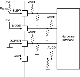
Hardware Interface

Hardware interface devices convert the four SPI pins into four resistor-configurable inputs which are GAIN, SLEW, MODE, and OCP.

This conversion lets the application designer configure the most common device settings by tying the pin logic high or logic low, or with a simple pullup or pulldown resistor. This removes the requirement for an SPI bus from the external controller. General fault information can still be obtained through the nFAULT pin.

  • The GAIN pin configures the gain of the current sense amplifier.
  • The SLEW pin configures the slew rate of the output voltage.
  • The MODE pin configures the PWM control mode.
  • The OCP/SR pin is used to configures the OCP level and active demagnetization modes.

For more information on the hardware interface, see the Section 8.3.10 section.
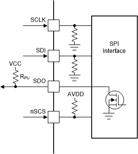
GUID-ECD1A14D-0863-4F0D-87D4-0CD667B2DF67-low.gifFigure 8-6 DRV8316R SPI Interface
GUID-20200906-CA0I-K4T8-TDWS-T3VPD3N6DPMZ-low.gifFigure 8-7 DRV8316T Hardware Interface