ZHCSJ76A March 2018 – April 2019 DRV8343-Q1
PRODUCTION DATA.
- 1 特性
- 2 应用
- 3 说明
- 4 修订历史记录
- 5 Device Comparison Table
- 6 Pin Configuration and Functions
- 7 Specifications
-
8 Detailed Description
- 8.1 Overview
- 8.2 Functional Block Diagram
- 8.3
Feature Description
- 8.3.1
Three Phase Smart Gate Drivers
- 8.3.1.1
PWM Control Modes
- 8.3.1.1.1 6x PWM Mode (PWM_MODE = 000b or MODE Pin Tied to AGND)
- 8.3.1.1.2 3x PWM Mode (PWM_MODE = 001b or MODE Pin = 18 kΩ to AGND)
- 8.3.1.1.3 1x PWM Mode (PWM_MODE = 010b or MODE Pin = 75 kΩ to AGND)
- 8.3.1.1.4 Independent Half-Bridge PWM Mode (PWM_MODE = 011b or MODE Pin is > 1.5 MΩ to AGND or Hi-Z)
- 8.3.1.1.5 Phases A and B are Independent Half-Bridges, Phase C is Independent FET (MODE = 100b)
- 8.3.1.1.6 Phases B and C are Independent Half-Bridges, Phase A is Independent FET (MODE = 101b or MODE Pin is 75 kΩ to DVDD)
- 8.3.1.1.7 Phases A is Independent Half-Bridge, Phases B and C are Independent FET (MODE = 110b or MODE Pin is 18 kΩ to DVDD)
- 8.3.1.1.8 Independent MOSFET Drive Mode (PWM_MODE = 111b or MODE Pin = 0.47 kΩ to DVDD)
- 8.3.1.2 Device Interface Modes
- 8.3.1.3 Gate Driver Voltage Supplies
- 8.3.1.4 Smart Gate Drive Architecture
- 8.3.1.1
PWM Control Modes
- 8.3.2 DVDD Linear Voltage Regulator
- 8.3.3 Pin Diagrams
- 8.3.4 Low-Side Current Sense Amplifiers
- 8.3.5
Gate Driver Protective Circuits
- 8.3.5.1 VM Supply Undervoltage Lockout (UVLO)
- 8.3.5.2 VCP Charge Pump Undervoltage Lockout (CPUV)
- 8.3.5.3 MOSFET VDS Overcurrent Protection (VDS_OCP)
- 8.3.5.4 VSENSE Overcurrent Protection (SEN_OCP)
- 8.3.5.5 Gate Driver Fault (GDF)
- 8.3.5.6 Thermal Warning (OTW)
- 8.3.5.7 Thermal Shutdown (OTSD)
- 8.3.5.8 Open Load Detection (OLD)
- 8.3.5.9 Offline Shorts Diagnostics
- 8.3.5.10 Reverse Supply Protection
- 8.3.1
Three Phase Smart Gate Drivers
- 8.4 Device Functional Modes
- 8.5 Programming
- 8.6
Register Maps
- 8.6.1 Status Registers
- 8.6.2
Control Registers
- 8.6.2.1 IC1 Control Register (Address = 0x04) [reset = 0x00]
- 8.6.2.2 IC2 Control Register (address = 0x05) [reset = 0x40]
- 8.6.2.3 IC3 Control Register (Address = 0x06) [reset = 0xFF]
- 8.6.2.4 IC4 Control Register (Address = 0x07) [reset = 0xFF]
- 8.6.2.5 IC5 Control Register (Address = 0x08) [reset = 0xFF]
- 8.6.2.6 IC6 Control Register (Address = 0x09) [reset = 0x99]
- 8.6.2.7 IC7 Control Register (Address = 0x0A) [reset = 0x99]
- 8.6.2.8 IC8 Control Register (Address = 0x0B) [reset = 0x99]
- 8.6.2.9 IC9 Control Register (Address = 0x0C) [reset = 0x2F]
- 8.6.2.10 IC10 Control Register (Address = 0x0D) [reset = 0x61]
- 8.6.2.11 IC11 Control Register (Address = 0x0E) [reset = 0x00]
- 8.6.2.12 IC12 Control Register (Address = 0x0F) [reset = 0x2A]
- 8.6.2.13 IC13 Control Register (Address = 0x10) [reset = 0x7F]
- 8.6.2.14 IC14 Control Register (Address = 0x10) [reset = 0x00]
- 9 Application and Implementation
- 10Power Supply Recommendations
- 11Layout
- 12器件和文档支持
- 13机械、封装和可订购信息
8.3.1.3 Gate Driver Voltage Supplies
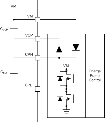
The voltage supply for the high-side gate driver is created using a doubler charge pump that operates from the VM voltage supply input. The charge pump lets the gate driver correctly bias the high-side MOSFET gate with respect to the source across a wide input supply voltage range. The charge pump is regulated to keep a fixed output voltage VVCP and supports an average output current IGATE_HS. The charge pump is continuously monitored for undervoltage events to prevent under-driven MOSFET conditions. The charge pump requires a ceramic capacitor between the VM and VCP pins to act as the storage capacitor. Additionally, a flying capacitor is required between the CPH and CPL pins.
 Figure 18. Charge Pump Architecture
 The voltage supply of the low-side gate driver is created using a linear regulator that operates from the VM voltage supply input. The linear regulator lets the gate driver correctly bias the low-side MOSFET gate with respect to ground. The linear regulator output is VGSL and supports an output current IGATE_LS.