ZHCSJ76A March 2018 – April 2019 DRV8343-Q1
PRODUCTION DATA.
- 1 特性
- 2 应用
- 3 说明
- 4 修订历史记录
- 5 Device Comparison Table
- 6 Pin Configuration and Functions
- 7 Specifications
-
8 Detailed Description
- 8.1 Overview
- 8.2 Functional Block Diagram
- 8.3
Feature Description
- 8.3.1
Three Phase Smart Gate Drivers
- 8.3.1.1
PWM Control Modes
- 8.3.1.1.1 6x PWM Mode (PWM_MODE = 000b or MODE Pin Tied to AGND)
- 8.3.1.1.2 3x PWM Mode (PWM_MODE = 001b or MODE Pin = 18 kΩ to AGND)
- 8.3.1.1.3 1x PWM Mode (PWM_MODE = 010b or MODE Pin = 75 kΩ to AGND)
- 8.3.1.1.4 Independent Half-Bridge PWM Mode (PWM_MODE = 011b or MODE Pin is > 1.5 MΩ to AGND or Hi-Z)
- 8.3.1.1.5 Phases A and B are Independent Half-Bridges, Phase C is Independent FET (MODE = 100b)
- 8.3.1.1.6 Phases B and C are Independent Half-Bridges, Phase A is Independent FET (MODE = 101b or MODE Pin is 75 kΩ to DVDD)
- 8.3.1.1.7 Phases A is Independent Half-Bridge, Phases B and C are Independent FET (MODE = 110b or MODE Pin is 18 kΩ to DVDD)
- 8.3.1.1.8 Independent MOSFET Drive Mode (PWM_MODE = 111b or MODE Pin = 0.47 kΩ to DVDD)
- 8.3.1.2 Device Interface Modes
- 8.3.1.3 Gate Driver Voltage Supplies
- 8.3.1.4 Smart Gate Drive Architecture
- 8.3.1.1
PWM Control Modes
- 8.3.2 DVDD Linear Voltage Regulator
- 8.3.3 Pin Diagrams
- 8.3.4 Low-Side Current Sense Amplifiers
- 8.3.5
Gate Driver Protective Circuits
- 8.3.5.1 VM Supply Undervoltage Lockout (UVLO)
- 8.3.5.2 VCP Charge Pump Undervoltage Lockout (CPUV)
- 8.3.5.3 MOSFET VDS Overcurrent Protection (VDS_OCP)
- 8.3.5.4 VSENSE Overcurrent Protection (SEN_OCP)
- 8.3.5.5 Gate Driver Fault (GDF)
- 8.3.5.6 Thermal Warning (OTW)
- 8.3.5.7 Thermal Shutdown (OTSD)
- 8.3.5.8 Open Load Detection (OLD)
- 8.3.5.9 Offline Shorts Diagnostics
- 8.3.5.10 Reverse Supply Protection
- 8.3.1
Three Phase Smart Gate Drivers
- 8.4 Device Functional Modes
- 8.5 Programming
- 8.6
Register Maps
- 8.6.1 Status Registers
- 8.6.2
Control Registers
- 8.6.2.1 IC1 Control Register (Address = 0x04) [reset = 0x00]
- 8.6.2.2 IC2 Control Register (address = 0x05) [reset = 0x40]
- 8.6.2.3 IC3 Control Register (Address = 0x06) [reset = 0xFF]
- 8.6.2.4 IC4 Control Register (Address = 0x07) [reset = 0xFF]
- 8.6.2.5 IC5 Control Register (Address = 0x08) [reset = 0xFF]
- 8.6.2.6 IC6 Control Register (Address = 0x09) [reset = 0x99]
- 8.6.2.7 IC7 Control Register (Address = 0x0A) [reset = 0x99]
- 8.6.2.8 IC8 Control Register (Address = 0x0B) [reset = 0x99]
- 8.6.2.9 IC9 Control Register (Address = 0x0C) [reset = 0x2F]
- 8.6.2.10 IC10 Control Register (Address = 0x0D) [reset = 0x61]
- 8.6.2.11 IC11 Control Register (Address = 0x0E) [reset = 0x00]
- 8.6.2.12 IC12 Control Register (Address = 0x0F) [reset = 0x2A]
- 8.6.2.13 IC13 Control Register (Address = 0x10) [reset = 0x7F]
- 8.6.2.14 IC14 Control Register (Address = 0x10) [reset = 0x00]
- 9 Application and Implementation
- 10Power Supply Recommendations
- 11Layout
- 12器件和文档支持
- 13机械、封装和可订购信息
8.3.4.4 MOSFET VDS Sense Mode (SPI Only)
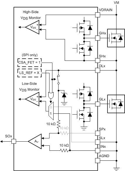
The current sense amplifiers on the DRV8343-Q1 SPI device can be configured to amplify the voltage across the external low-side MOSFET VDS. This configuration lets the external controller measure the voltage drop across the MOSFET RDS(on) without the shunt resistor and then calculate the half-bridge current level. This setting is not available in the H/W device.
To enable this mode set the CSA_FET bit to 1. The positive input of the amplifier is then internally connected to the DLx pin with an internal clamp to prevent high voltage on the DLx pin from damaging the sense amplifier inputs. During this mode of operation, the SPx pins should stay disconnected. When the CSA_FET bit is set to 1, the negative reference for the low-side VDS monitor is automatically set to the SNx pin, regardless of the state of the state of the LS_REF bit. This setting is implemented to prevent disabling of the low-side VDS monitor.
If the system operates in MOSFET VDS current sense mode, route the DLx and SNx pins with Kelvin connections across the drain and source of the external low-side MOSFETs.
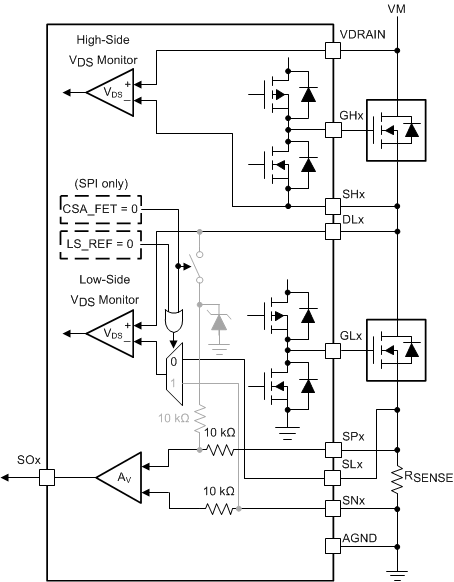
 Figure 36. Resistor Sense Configuration
  Figure 37. VDS Current Sense Mode
 When operating in MOSFET VDS current sense mode, the amplifier is enabled at the end of the tDRIVE time. At this time, the amplifier input is connected to the DLx pin, and the SOx output is valid. When the low-side MOSFET receives a signal to turn off, the amplifier inputs, SPx and SNx, are shorted together internally.