ZHCSR67 July 2020 DRV8353M
PRODUCTION DATA
- 1 特性
- 2 应用
- 3 说明
- 4 Revision History
- 5 Device Comparison Table
- 6 Pin Configuration and Functions
- 7 Absolute Maximum Ratings
- 8 ESD Ratings
- 9 Recommended Operating Conditions
- 10Thermal Information
- 11Electrical Characteristics
- 12SPI Timing Requirements
-
13Detailed Description
- 13.1 Overview
- 13.2 Functional Block Diagram
- 13.3
Feature Description
- 13.3.1 Three Phase Smart Gate Drivers
- 13.3.2 DVDD Linear Voltage Regulator
- 13.3.3 Pin Diagrams
- 13.3.4 Low-Side Current-Shunt Amplifiers
- 13.3.5
Gate Driver Protective Circuits
- 13.3.5.1 VM Supply and VDRAIN Undervoltage Lockout (UVLO)
- 13.3.5.2 VCP Charge-Pump and VGLS Regulator Undervoltage Lockout (GDUV)
- 13.3.5.3 MOSFET VDS Overcurrent Protection (VDS_OCP)
- 13.3.5.4 VSENSE Overcurrent Protection (SEN_OCP)
- 13.3.5.5 Gate Driver Fault (GDF)
- 13.3.5.6 Overcurrent Soft Shutdown (OCP Soft)
- 13.3.5.7 Thermal Warning (OTW)
- 13.3.5.8 Thermal Shutdown (OTSD)
- 13.3.5.9 Fault Response Table
- 13.4 Device Functional Modes
- 13.5 Programming
- 13.6
Register Maps
- 13.6.1 Status Registers
- 13.6.2
Control Registers
- 13.6.2.1 Driver Control Register (address = 0x02h)
- 13.6.2.2 Gate Drive HS Register (address = 0x03h)
- 13.6.2.3 Gate Drive LS Register (address = 0x04h)
- 13.6.2.4 OCP Control Register (address = 0x05h)
- 13.6.2.5 CSA Control Register (address = 0x06h)
- 13.6.2.6 Driver Configuration Register (address = 0x07h)
-
14Application and Implementation
- 14.1 Application Information
- 14.2
Typical Application
- 14.2.1
Primary Application
- 14.2.1.1 Design Requirements
- 14.2.1.2 Detailed Design Procedure
- 14.2.1.3 Application Curves
- 14.2.1
Primary Application
- 15Power Supply Recommendations
- 16Layout
- 17Device and Documentation Support
- 18Mechanical, Packaging, and Orderable Information
13.3.1.4.2 TDRIVE: MOSFET Gate Drive Control
The TDRIVE component is an integrated gate-drive state machine that provides automatic dead time insertion through switching handshaking, parasitic dV/dt gate turnon prevention, and MOSFET gate-fault detection.
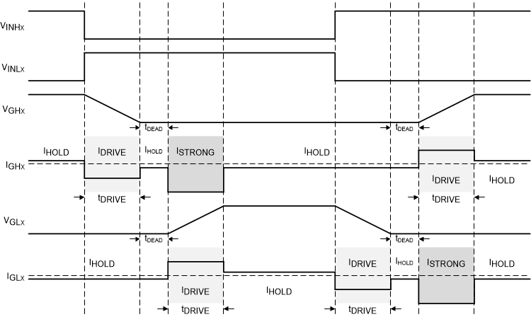
The first component of the TDRIVE state machine is automatic dead-time insertion. Dead time is period of time between the switching of the external high-side and low-side MOSFETs to make sure that they do not cross conduct and cause shoot-through. The DRV8353M family of devices use VGS voltage monitors to measure the MOSFET gate-to-source voltage and determine the correct time to switch instead of relying on a fixed time value. This feature allows the gate-driver dead time to adjust for variation in the system such a temperature drift and variation in the MOSFET parameters. An additional digital dead time (tDEAD) can be inserted and is adjustable through the registers on SPI devices.
The automatic dead-time insertion has a limitation when the gate driver is transitioning from high-side MOSFET on to low-side MOSFET on when the phase current is coming into the external half-bridge. In this case, the high-side diode will conduct during the dead-time and hold up the switch-node voltage to VDRAIN. In this case, an additional delay of approximately 100-200 ns is introduced into the dead-time handshake. This is introduced due to the need to discharge the voltage present on the internal VGS detection circuit.
The second component focuses on parasitic dV/dt gate turnon prevention. To implement this, the TDRIVE state machine enables a strong pulldown ISTRONG current on the opposite MOSFET gate whenever a MOSFET is switching. The strong pulldown last for the TDRIVE duration. This feature helps remove parasitic charge that couples into the MOSFET gate when the half-bridge switch-node voltage slews rapidly.
The third component implements a gate-fault detection scheme to detect pin-to-pin solder defects, a MOSFET gate failure, or a MOSFET gate stuck-high or stuck-low voltage condition. This implementation is done with a pair of VGS gate-to-source voltage monitors for each half-bridge gate driver. When the gate driver receives a command to change the state of the half-bridge it starts to monitor the gate voltage of the external MOSFET. If at the end of the tDRIVE period the VGS voltage has not reached the correct threshold the gate driver will report a fault. To make sure that a false fault is not detected, a tDRIVE time should be selected that is longer than the time required to charge or discharge the MOSFET gate. The tDRIVE time does not increase the PWM time and will terminate if another PWM command is received while active. Additional details on the TDRIVE settings are described in the Section 13.6 section for SPI devices and in the Section 13.3.3 section for hardware interface devices.
Figure 13-14 shows an example of the TDRIVE state machine in operation.
 Figure 13-14 TDRIVE State Machine