ZHCSND1A November 2020 – May 2022 DRV8434
PRODUCTION DATA
- 1 特性
- 2 应用
- 3 说明
- 4 Revision History
- 5 Pin Configuration and Functions
- 6 规格
- 7 详细说明
- 8 Application and Implementation
- 9 Power Supply Recommendations
- 10Layout
- 11Device and Documentation Support
- 12Mechanical, Packaging, and Orderable Information
封装选项
机械数据 (封装 | 引脚)
散热焊盘机械数据 (封装 | 引脚)
- RGE|24
订购信息
7.3.9 Logic Level, Tri-Level and Quad-Level Pin Diagrams
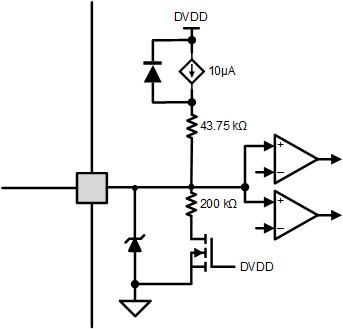
Figure 7-15 shows the input structure for M0, DECAY0 and ENABLE pins.
 Figure 7-15 Tri-Level Input Pin Diagram
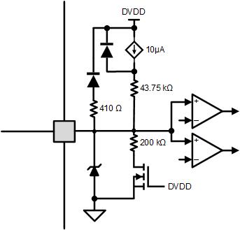
Figure 7-16 shows the input structure for DECAY1 pin.
 Figure 7-16 DECAY1 Pin Diagram
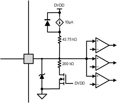
Figure 7-17 shows the input structure for M1 and TOFF pins.
 Figure 7-17 Quad-Level Input Pin Diagram
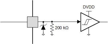
Figure 7-18 shows the input structure for STEP, DIR and nSLEEP pins.
 Figure 7-18 Logic-Level Input Pin Diagram