ZHCSE26B August 2015 – July 2016 DRV8871
PRODUCTION DATA.
10 Layout
10.1 Layout Guidelines
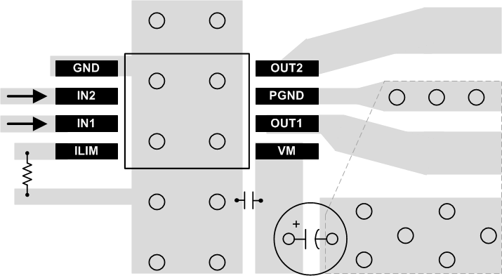
The bulk capacitor should be placed to minimize the distance of the high-current path through the motor driver device. The connecting metal trace widths should be as wide as possible, and numerous vias should be used when connecting PCB layers. These practices minimize inductance and allow the bulk capacitor to deliver high current.
Small-value capacitors should be ceramic, and placed closely to device pins.
The high-current device outputs should use wide metal traces.
The device thermal pad should be soldered to the PCB top-layer ground plane. Multiple vias should be used to connect to a large bottom-layer ground plane. The use of large metal planes and multiple vias help dissipate the I2 × RDS(on) heat that is generated in the device.
10.2 Layout Example
Recommended layout and component placement is shown in Figure 15
 Figure 15. Layout Recommendation
10.3 Thermal Considerations
The DRV8871 device has thermal shutdown (TSD) as described in the Thermal Shutdown (TSD) section. If the die temperature exceeds approximately 175°C, the device is disabled until the temperature drops below the temperature hysteresis level.
Any tendency of the device to enter TSD is an indication of either excessive power dissipation, insufficient heatsinking, or too high of an ambient temperature.
10.4 Power Dissipation
Power dissipation in the DRV8871 device is dominated by the power dissipated in the output FET resistance, RDS(on). Use the equation in the Drive Current section to calculate the estimated average power dissipation when driving a load.
Note that at startup, the current is much higher than normal running current; this peak current and its duration must be also be considered.
The maximum amount of power that can be dissipated in the device is dependent on ambient temperature and heatsinking.
NOTE
RDS(on) increases with temperature, so as the device heats, the power dissipation increases. This fact must be taken into consideration when sizing the heatsink.
The power dissipation of the DRV8871 device is a function of RMS motor current and the FET resistance (RDS(ON)) of each output.

For this example, the ambient temperature is 58°C, and the junction temperature reaches 80°C. At 58°C, the sum of RDS(ON) is about 0.72 Ω. With an example motor current of 0.8 A, the dissipated power in the form of heat will be 0.8 A2 × 0.72 Ω = 0.46 W.
The temperature that the DRV8871 device reaches depends on the thermal resistance to the air and PCB. It is important to solder the device PowerPAD to the PCB ground plane, with vias to the top and bottom board layers, in order dissipate heat into the PCB and reduce the device temperature. In the example used here, the DRV8871 device had an effective thermal resistance RθJA of 48°C/W, and:

10.4.1 Heatsinking
The PowerPAD package uses an exposed pad to remove heat from the device. For proper operation, this pad must be thermally connected to copper on the PCB to dissipate heat. On a multi-layer PCB with a ground plane, this connection can be accomplished by adding a number of vias to connect the thermal pad to the ground plane.
On PCBs without internal planes, a copper area can be added on either side of the PCB to dissipate heat. If the copper area is on the opposite side of the PCB from the device, thermal vias are used to transfer the heat between top and bottom layers.
For details about how to design the PCB, refer to PowerPAD™ Thermally Enhanced Package (SLMA002) and PowerPAD Made Easy™ (SLMA004), available at www.ti.com. In general, the more copper area that can be provided, the more power can be dissipated.