ZHCSFQ0 November   2016 DRV8872-Q1

PRODUCTION DATA.  

  1. 特性
  2. 应用范围
  3. 说明
  4. 修订历史记录
  5. Pin Configuration and Functions
  6. Specifications
    1. 6.1 Absolute Maximum Ratings
    2. 6.2 ESD Ratings
    3. 6.3 Recommended Operating Conditions
    4. 6.4 Thermal Information
    5. 6.5 Electrical Characteristics
    6. 6.6 Typical Characteristics
  7. Detailed Description
    1. 7.1 Overview
    2. 7.2 Functional Block Diagram
    3. 7.3 Feature Description
      1. 7.3.1 Bridge Control
      2. 7.3.2 Sleep Mode
      3. 7.3.3 Current Regulation
      4. 7.3.4 Dead Time
      5. 7.3.5 Protection Circuits
        1. 7.3.5.1 VM Undervoltage Lockout (UVLO)
        2. 7.3.5.2 Overcurrent Protection (OCP)
        3. 7.3.5.3 Thermal Shutdown (TSD)
    4. 7.4 Device Functional Modes
      1. 7.4.1 PWM With Current Regulation
      2. 7.4.2 PWM Without Current Regulation
      3. 7.4.3 Static Inputs With Current Regulation
      4. 7.4.4 VM Control
  8. Application and Implementation
    1. 8.1 Application Information
    2. 8.2 Typical Application
      1. 8.2.1 Design Requirements
      2. 8.2.2 Detailed Design Procedure
        1. 8.2.2.1 Motor Voltage
        2. 8.2.2.2 Drive Current
        3. 8.2.2.3 Sense Resistor
      3. 8.2.3 Application Curves
  9. Power Supply Recommendations
    1. 9.1 Bulk Capacitance
  10. 10Layout
    1. 10.1 Layout Guidelines
    2. 10.2 Layout Example
    3. 10.3 Thermal Considerations
    4. 10.4 Power Dissipation
      1. 10.4.1 Heatsinking
  11. 11器件和文档支持
    1. 11.1 文档支持
      1. 11.1.1 相关文档
    2. 11.2 接收文档更新通知
    3. 11.3 社区资源
    4. 11.4 商标
    5. 11.5 静电放电警告
    6. 11.6 Glossary
  12. 12机械、封装和可订购信息

封装选项

机械数据 (封装 | 引脚)
散热焊盘机械数据 (封装 | 引脚)
订购信息

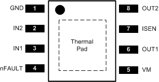
Pin Configuration and Functions

DDA Package
8-Pin HSOP With Exposed Thermal Pad
Top View
DRV8872-Q1 po_lvscz0.gif

Pin Functions

PIN TYPE DESCRIPTION
NAME NO.
GND 1 PWR Logic ground Connect to board ground.
IN1 3 I Logic inputs Controls the H-bridge output. Has internal pulldowns. (See Table 1.)
IN2 2
ISEN 7 PWR High-current ground path If using current regulation, connect ISEN to a resistor (low-value, high-power-rating) to ground. If not using current regulation, connect ISEN directly to ground.
nFAULT 4 OD Fault status (open-drain) Low-level indicates UVLO, TSD, or OCP fault. Connect to a pullup resistor.
OUT1 6 O H-bridge outputs Connect directly to the motor, or other inductive load.
OUT2 8
VM 5 PWR 6.8-V to 45-V power supply Connect a 0.1-µF bypass capacitor to ground, as well as sufficient bulk capacitance, rated for the VM voltage.
PAD Thermal pad Connect to board ground. For good thermal dissipation, use large ground planes on multiple layers, and multiple nearby vias connecting those planes.