ZHCSRO2 February   2023 DS160PR1601

PRODUCTION DATA  

  1. 特性
  2. 应用
  3. 说明
  4. Revision History
  5. Pin Configuration and Functions
  6. Specifications
    1. 6.1 Absolute Maximum Ratings
    2. 6.2 ESD and Latchup Ratings
    3. 6.3 Recommended Operating Conditions
    4. 6.4 Thermal Information
    5. 6.5 DC Electrical Characteristics
    6. 6.6 High Speed Electrical Characteristics
    7. 6.7 SMBUS/I2C Timing Charateristics
    8. 6.8 Typical Characteristics
    9. 6.9 Typical Jitter Characteristics
  7. Detailed Description
    1. 7.1 Overview
    2. 7.2 Functional Block Diagram
    3. 7.3 Control and Configuration Interface
      1. 7.3.1 Pin Configurations for Lanes
        1. 7.3.1.1 Five-Level Control Inputs
      2. 7.3.2 SMBUS/I2C Register Control Interface
      3. 7.3.3 SMBus/I 2 C Primary Mode Configuration (EEPROM Self Load)
    4. 7.4 Feature Description
      1. 7.4.1 Linear Equalization
      2. 7.4.2 Flat-Gain
      3. 7.4.3 Analog EyeScan
      4. 7.4.4 Receiver Detect State Machine
      5. 7.4.5 Integrated Capacitors
    5. 7.5 Device Functional Modes
      1. 7.5.1 Active PCIe Mode
      2. 7.5.2 Active Buffer Mode
      3. 7.5.3 Standby Mode
  8. Application and Implementation
    1. 8.1 Application Information
    2. 8.2 Typical Applications
      1. 8.2.1 PCIe x16 Lane Configuration
        1. 8.2.1.1 Design Requirements
        2. 8.2.1.2 Detailed Design Procedure
        3. 8.2.1.3 Application Curves
    3. 8.3 Power Supply Recommendations
    4. 8.4 Layout
      1. 8.4.1 Layout Guidelines
      2. 8.4.2 Layout Example
  9. Device and Documentation Support
    1. 9.1 Documentation Support
      1. 9.1.1 Related Documentation
    2. 9.2 接收文档更新通知
    3. 9.3 支持资源
    4. 9.4 Trademarks
    5. 9.5 静电放电警告
    6. 9.6 术语表
  10. 10Mechanical, Packaging, and Orderable Information

封装选项

机械数据 (封装 | 引脚)
散热焊盘机械数据 (封装 | 引脚)
订购信息

Pin Configurations for Lanes

The DS160PR1601 has 16 data lanes with 16-Tx channels and 16-Rx channels. The data channels are grouped for I2C configurations and PCIe state machine grouping as shown in #FIG_G1Z_YVZ_CPB using xADDRx and PDx pins. Table 7-1 defines the channel grouping.
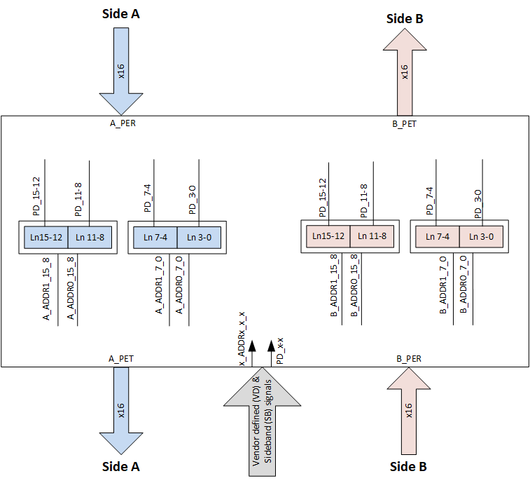
GUID-20210330-CA0I-2FJ3-HJVZ-0MK3XLFMLSCT-low.gif Figure 7-1 Pin Configurations for Lanes
Table 7-1 Definition of PDx and xADDRx pins
Pin Name Description

PD_15-12

PD_11-8

PD_7-4

PD_3-0

Active in all device control modes. The pin has internal 1-MΩ weak pulldown resistor. The pin triggers PCIe RX detect state machine when toggled.

  • High: power down
  • Low: power up normal operation.

Each PD pin sets control for a bank of 8 lanes (4 from Side A and 4 from Side B) to provide flexibility for x4 and x8 bifurcation:

  • PD_15-12: Lanes 15-12, both Side A and B
  • PD_11-8: Lanes 11-8, both Side A and B
  • PD_7-4: Lanes 7-4, both Side A and B
  • PD_3-0: Lanes 3-0, both Side A and B

PCIe hot plug insertion implementation varies from system to system. One way to implement will be to use CEM interface PRSNT# signal. For PCIe x16 application all four PD signals can be shorted together and connect to CEM interface PRSNT# signal.

A_ADDR1_15-8

A_ADDR0_15-8

A_ADDR1_7-0

A_ADDR0_7-0

B_ADDR1_15-8

B_ADDR0_15-8

B_ADDR1_7-0

B_ADDR0_7-0

5-level input pins as implemented by pull-down resistor on the pin according to Table 7-5.

These pins are sampled at device power-up only. Sets SMBus / I2C secondary address according to Table 7-3. Each set of ADDR1 and ADDR0 pins defines the addresses for bank of 8 lanes:

  • A_ADDR1_15-8, A_ADDR0_15-8: Lanes 15-8 of Side A
  • A_ADDR1_7-0, A_ADDR0_7-0: Lanes 7-0 of Side A
  • B_ADDR1_15-8, B_ADDR0_15-8: Lanes 15-8 of Side B
  • B_ADDR1_7-0, B_ADDR0_7-0: Lanes 7-0 of Side B

#FIG_G1Z_YVZ_CPB shows how I2C secondary addresses are accessed for specific lanes.