ZHCSDR2A April   2015  – October 2024 FDC1004-Q1

PRODUCTION DATA  

  1.   1
  2. 特性
  3. 应用
  4. 说明
  5. Pin Configuration and Functions
  6. Specifications
    1. 5.1 Absolute Maximum Ratings
    2. 5.2 ESD Ratings
    3. 5.3 Recommended Operating Conditions
    4. 5.4 Thermal Information
    5. 5.5 Electrical Characteristics
    6. 5.6 I2C Interface Voltage Level
    7. 5.7 I2C Interface Timing
    8. 5.8 Typical Characteristics
  7. Detailed Description
    1. 6.1 Overview
    2. 6.2 Functional Block Diagram
    3. 6.3 Feature Description
      1. 6.3.1 The Shield
      2. 6.3.2 The CAPDAC
      3. 6.3.3 Capacitive System Offset Calibration
      4. 6.3.4 Capacitive Gain Calibration
    4. 6.4 Device Functional Modes
      1. 6.4.1 Single Ended Measurement
      2. 6.4.2 Differential Measurement
    5. 6.5 Programming
      1. 6.5.1 Serial Bus Address
      2. 6.5.2 Read/Write Operations
      3. 6.5.3 Device Usage
        1. 6.5.3.1 Measurement Configuration
        2. 6.5.3.2 Triggering Measurements
        3. 6.5.3.3 Wait for Measurement Completion
        4. 6.5.3.4 Read of Measurement Result
    6. 6.6 Register Maps
      1. 6.6.1 Registers
        1. 6.6.1.1 Capacitive Measurement Registers
      2. 6.6.2 Measurement Registers
      3. 6.6.3 Measurement Configuration Registers
      4. 6.6.4 FDC Configuration Register
      5. 6.6.5 Offset Calibration Registers
      6. 6.6.6 Gain Calibration Registers
      7. 6.6.7 Manufacturer ID Register
      8. 6.6.8 Device ID Register
  8. Applications and Implementation
    1. 7.1 Application Information
      1. 7.1.1 Liquid Level Sensor
    2. 7.2 Typical Application
      1. 7.2.1 Design Requirements
      2. 7.2.2 Detailed Design Procedure
      3. 7.2.3 Application Curve
    3. 7.3 Best Design Practices
    4. 7.4 Initialization Set Up
    5. 7.5 Power Supply Recommendations
    6. 7.6 Layout
      1. 7.6.1 Layout Guidelines
      2. 7.6.2 Layout Example
  9. Device and Documentation Support
    1. 8.1 Documentation Support
      1. 8.1.1 Related Documentation
    2. 8.2 接收文档更新通知
    3. 8.3 支持资源
    4. 8.4 Trademarks
    5. 8.5 静电放电警告
    6. 8.6 术语表
  10. Revision History
  11. 10Mechanical, Packaging, and Orderable Information

封装选项

机械数据 (封装 | 引脚)
散热焊盘机械数据 (封装 | 引脚)
订购信息

Differential Measurement

When the FDC1004-Q1 is used for interfacing to a differential capacitive sensor, each of the two input capacitances must be less than 115pF. In this configuration the CAPDAC is disabled. Keep the absolute value of the difference between the two input capacitances below 15pF to avoid introducing errors in the measurement. In differential measurements, SHLD1 is assigned to CHn and SHLD2 is assigned to CHm, where n < m. For instance in the measurement CIN1 – CIN2, where CHA = CIN1 and CHB = CIN2 (see Table 6-4), SHDL1 is assigned to CIN1 and SHDL2 is to CIN2. Differential sensors made with S1 versus S3 and S2 versus S4 are shown below in Figure 6-3. S1 and S2 are alternatively connected to CHA and the S3 and S4 are alternatively connected to CHB, the shield signals are connected as explained in previous paragraph. The FDC1004-Q1 performs a differential measurement when CHB field of the Measurements Configuration Registers (refer to Table 6-4) is less than to b100.

This configuration is very useful in applications where environment conditions need to be tracked. The differential measurement between the main electrode and the environment electrode makes the measurement independent of the environment conditions.
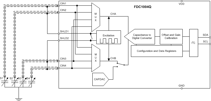
FDC1004-Q1 Differential ConfigurationFigure 6-3 Differential Configuration