ZHCSE92 September 2015 INA188
UNLESS OTHERWISE NOTED, this document contains PRODUCTION DATA.
7 Detailed Description
7.1 Overview
The INA188 is a monolithic instrumentation amplifier (INA) based on the 36-V, precision zero-drift OPA188 (operational amplifier) core. The INA188 also integrates laser-trimmed resistors to ensure excellent common-mode rejection and low gain error. The combination of the zero-drift amplifier core and the precision resistors allows this device to achieve outstanding dc precision and makes the INA188 ideal for many high-voltage industrial applications.
7.2 Functional Block Diagram
7.3 Feature Description
7.3.1 Inside the INA188
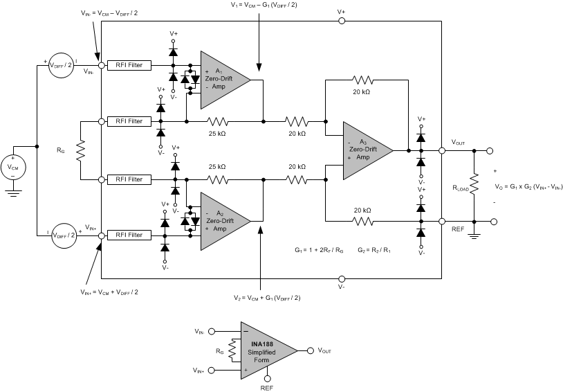
The Functional Block Diagram section provides a detailed diagram for the INA188, including the ESD protection and radio frequency interference (RFI) filtering. Instrumentation amplifiers are commonly represented in a simplified form, as shown in Figure 47.
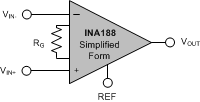 Figure 47. INA Simplified Form
A brief description of the internal operation is as follows:
The differential input voltage applied across RG causes a signal current to flow through the RG resistor and both RF resistors. The output difference amplifier (A3) removes the common-mode component of the input signal and refers the output signal to the REF pin.
The equations shown in the Functional Block Diagram section describe the output voltages of A1 and A2. Understanding the internal node voltages is useful to avoid saturating the device and to ensure proper device operation.
7.3.2 Setting the Gain
The gain of the INA188 is set by a single external resistor, RG, connected between pins 1 and 8. The value of RG is selected according to Equation 1:

Table 1 lists several commonly-used gains and resistor values. The 50-kΩ term in Equation 1 comes from the sum of the two internal 25-kΩ feedback resistors. These on-chip resistors are laser-trimmed to accurate absolute values. The accuracy and temperature coefficients of these resistors are included in the gain accuracy and drift specifications of the INA188.
Table 1. Commonly-Used Gains and Resistor Values
| DESIRED GAIN | RG (Ω) | NEAREST 1% RG (Ω) |
|---|---|---|
| 1 | NC(1) | NC |
| 2 | 50k | 49.9k |
| 5 | 12.5k | 12.4k |
| 10 | 5.556k | 5.49k |
| 20 | 2.632k | 2.61k |
| 50 | 1.02k | 1.02k |
| 100 | 505.1 | 511 |
| 200 | 251.3 | 249 |
| 500 | 100.2 | 100 |
| 1000 | 50.05 | 49.9 |
7.3.2.1 Gain Drift
The stability and temperature drift of the external gain setting resistor, RG, also affects gain. The contribution of RG to gain accuracy and drift can be determined from Equation 1.
The best gain drift of 5 ppm/℃ can be achieved when the INA188 uses G = 1 without RG connected. In this case, gain drift is limited only by the slight mismatch of the temperature coefficient of the integrated 20-kΩ resistors in the differential amplifier (A3). At gains greater than 1, gain drift increases as a result of the individual drift of the 25-kΩ resistors in the feedback of A1 and A2, relative to the drift of the external gain resistor RG. The low temperature coefficient of the internal feedback resistors significantly improves the overall temperature stability of applications using gains greater than 1 V/V over competing alternate solutions.
Low resistor values required for high gain can make wiring resistance important. Sockets add to the wiring resistance and contribute additional gain error (such as a possible unstable gain error) at gains of approximately 100 or greater. To ensure stability, avoid parasitic capacitance of more than a few picofarads at RG connections. Careful matching of any parasitics on both RG pins maintains optimal CMRR over frequency; see Typical Characteristics curve, Figure 17.
7.3.3 Zero Drift Topology
7.3.3.1 Internal Offset Correction
Figure 48 shows a simple representation of the proprietary zero-drift architecture for one of the three amplifiers that comprise the INA188. These high-precision input amplifiers enable very low dc error and drift as a result of a modern chopper technology with an embedded synchronous filter that removes nearly all chopping noise. The chopping frequency is approximately 750 kHz. This amplifier is zero-corrected every 3 μs using a proprietary technique. This design has no aliasing.
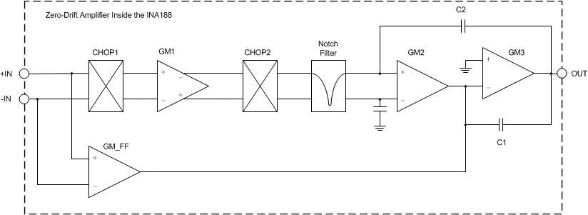 Figure 48. Zero-Drift Amplifier Functional Block Diagram
7.3.3.2 Noise Performance
This zero-drift architecture reduces flicker (1/f) noise to a minimum, and therefore enables the precise measurement of small dc-signals with high resolution, accuracy, and repeatability. The auto-calibration technique used by the INA188 results in reduced low-frequency noise, typically only 12 nV/√Hz (at G = 100). The spectral noise density is detailed in Figure 53. Low-frequency noise of the INA188 is approximately 0.25 μVPP measured from 0.1 Hz to 10 Hz (at G = 100).
7.3.3.3 Input Bias Current Clock Feedthrough
Zero-drift amplifiers, such as the INA188, use switching on their inputs to correct for the intrinsic offset and drift of the amplifier. Charge injection from the integrated switches on the inputs can introduce very short transients in the input bias current of the amplifier. The extremely short duration of these pulses prevents them from being amplified; however, the pulses can be coupled to the output of the amplifier through the feedback network. The most effective method to prevent transients in the input bias current from producing additional noise at the amplifier output is to use a low-pass filter (such as an RC network).
7.3.4 EMI Rejection
The INA188 uses integrated electromagnetic interference (EMI) filtering to reduce the effects of EMI from sources (such as wireless communications) and densely-populated boards with a mix of analog signal-chain and digital components. The INA188 is specifically designed to minimize susceptibility to EMI by incorporating an internal low-pass filter. Depending on the end-system requirements, additional EMI filters may be required near the signal inputs of the system, as well as incorporating known good practices such as using short traces, low-pass filters, and damping resistors combined with parallel and shielded signal routing. Texas Instruments developed a method to accurately measure the immunity of an amplifier over a broad frequency spectrum, extending from 10 MHz to 6 GHz. This method uses an EMI rejection ratio (EMIRR) to quantify the INA188 ability to reject EMI. Figure 49 and Figure 50 show the INA188 EMIRR graph for both differential and common-mode EMI rejection across this frequency range. Table 2 shows the EMIRR values for the INA188 at frequencies commonly encountered in real-world applications. Applications listed in Table 2 can be centered on or operated near the particular frequency shown.
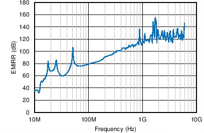
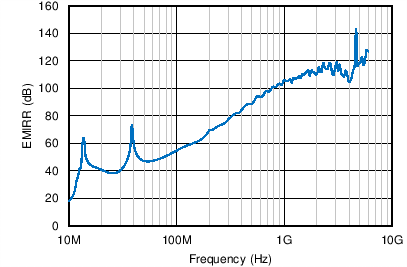
Table 2. INA188 EMIRR for Frequencies of Interest
| FREQUENCY | APPLICATION OR ALLOCATION | DIFFERENTIAL (IN-P) EMIRR |
COMMON-MODE EMIRR |
|---|---|---|---|
| 400 MHz | Mobile radio, mobile satellite, space operation, weather, radar, ultrahigh-frequency (UHF) applications | 83 dB | 101 dB |
| 900 MHz | Global system for mobile communications (GSM) applications, radio communication, navigation, GPS (to 1.6 GHz), GSM, aeronautical mobile, UHF applications | 103 dB | 118 dB |
| 1.8 GHz | GSM applications, mobile personal communications, broadband, satellite, L-band (1 GHz to 2 GHz) |
112 dB | 125 dB |
| 2.4 GHz | 802.11b, 802.11g, 802.11n, Bluetooth®, mobile personal communications, industrial, scientific and medical (ISM) radio band, amateur radio and satellite, S-band (2 GHz to 4 GHz) | 114 dB | 123 dB |
| 3.6 GHz | Radiolocation, aero communication and navigation, satellite, mobile, S-band | 110 dB | 121 dB |
| 5.0 GHz | 802.11a, 802.11n, aero communication and navigation, mobile communication, space and satellite operation, C-band (4 GHz to 8 GHz) | 119 dB | 123 dB |
7.3.5 Input Protection and Electrical Overstress
Designers often ask questions about the capability of an amplifier to withstand electrical overstress. These questions tend to focus on the device inputs, but can involve the supply voltage pins or even the output pin. Each of these different pin functions have electrical stress limits determined by the voltage breakdown characteristics of the particular semiconductor fabrication process and specific circuits connected to the pin. Additionally, internal ESD protection is built into these circuits to protect them from accidental ESD events both before and during product assembly.
Having a good understanding of this basic ESD circuitry and its relevance to an electrical overstress event is helpful. The Functional Block Diagram section illustrates the ESD circuits contained in the INA188. The ESD protection circuitry involves several current-steering diodes connected from the input and output pins and routed back to the internal power-supply lines. This protection circuitry is intended to remain inactive during normal circuit operation.
The input pins of the INA188 are protected with internal diodes connected to the power-supply rails. These diodes clamp the applied signal to prevent the input circuitry from being damaged. If the input signal voltage can exceed the power supplies by more than 0.3 V, limit the input signal current to less than 10 mA to protect the internal clamp diodes. This current limiting can generally be done with a series input resistor. Some signal sources are inherently current-limited and do not require limiting resistors.
7.3.6 Input Common-Mode Range
The linear input voltage range of the INA188 input circuitry extends from 100 mV inside the negative supply voltage to 1.5 V below the positive supply, and maintains 84-dB (minimum) common-mode rejection throughout this range. The common-mode range for most common operating conditions is best calculated using the INA common-mode range calculating tool. The INA188 can operate over a wide range of power supplies and VREF configurations, thus providing a comprehensive guide to common-mode range limits for all possible conditions is impractical.
The most commonly overlooked overload condition occurs when a circuit exceeds the output swing of A1 and A2, which are internal circuit nodes that cannot be measured. Calculating the expected voltages at the output of A1 and A2 (see the Functional Block Diagram section) provides a check for the most common overload conditions. The designs of A1 and A2 are identical and the outputs can swing to within approximately 250 mV of the power-supply rails. For example, when the A2 output is saturated, A1 can continue to be in linear operation, responding to changes in the noninverting input voltage. This difference can give the appearance of linear operation but the output voltage is invalid.
7.4 Device Functional Modes
7.4.1 Single-Supply Operation
The INA188 can be used on single power supplies of 4 V to 36 V. Use the output REF pin to level shift the internal output voltage into a linear operating condition. Ideally, connecting the REF oin to a potential that is mid-supply avoids saturating the output of the input amplifiers (A1 and A2). Actual output voltage swing is limited to 250 mV above ground when the load is referred to ground. The typical characteristic curves, Output Voltage Swing vs Output Current (Figure 19 to Figure 22) illustrates how the output voltage swing varies with output current. See the Driving the Reference Pin section for information on how to adequately drive the reference pin.
With single-supply operation, VIN+ and VIN– must both be 0.1 V above ground for linear operation. For instance, the inverting input cannot be connected to ground to measure a voltage connected to the noninverting input.
7.4.2 Offset Trimming
Most applications require no external offset adjustment; however, if necessary, adjustments can be made by applying a voltage to the REF pin. Figure 51 shows an optional circuit for trimming the output offset voltage. The voltage applied to the REF pin is summed at the output. The op amp buffer provides low impedance at the REF pin to preserve good common-mode rejection.
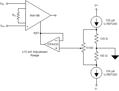 Figure 51. Optional Trimming of the Output Offset Voltage
7.4.3 Input Bias Current Return Path
The input impedance of the INA188 is extremely high—approximately 20 GΩ. However, a path must be provided for the input bias current of both inputs. This input bias current is typically 750 pA. High input impedance means that this input bias current changes very little with varying input voltage.
Input circuitry must provide a path for this input bias current for proper operation. Figure 52 shows various provisions for an input bias current path. Without a bias current path, the inputs float to a potential that exceeds the common-mode range of the INA188, and the input amplifiers saturate. If the differential source resistance is low, the bias current return path can be connected to one input (as shown in the thermocouple example in Figure 52). With a higher source impedance, using two equal resistors provides a balanced input with possible advantages of a lower input offset voltage as a result of bias current and better high-frequency common-mode rejection.
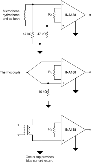 Figure 52. Providing an Input Common-Mode Current Path
7.4.4 Driving the Reference Pin
The output voltage of the INA188 is developed with respect to the voltage on the reference pin. Often, the reference pin (pin 5) is connected to the low-impedance system ground in dual-supply operation. In single-supply operation, offsetting the output signal to a precise mid-supply level (for example, 2.5 V in a 5-V supply environment) can be useful. To accomplish this, a voltage source can be tied to the REF pin to level-shift the output so that the INA188 can drive a single-supply analog-to-digital converter (ADC).
For best performance, keep the source impedance to the REF pin below 5 Ω. As illustrated in the Functional Block Diagram section, the reference pin is internally connected to a 20-kΩ resistor. Additional impedance at the REF pin adds to this 20-kΩ resistor. The imbalance in the resistor ratios results in degraded common-mode rejection ratio (CMRR).
Figure 53 shows two different methods of driving the reference pin with low impedance. The OPA330 is a low-power, chopper-stabilized amplifier, and therefore offers excellent stability over temperature. The OPA330 is available in a space-saving SC70 and an even smaller chip-scale package. The REF3225 is a precision reference in a small SOT23-6 package.
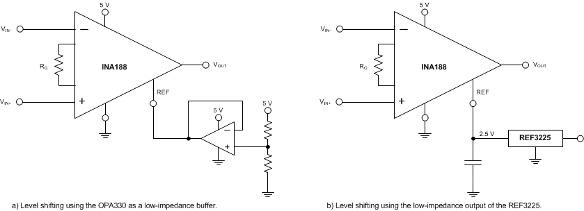 Figure 53. Options for Low-Impedance Level Shifting
7.4.5 Error Sources Example
Most modern signal-conditioning systems calibrate errors at room temperature. However, calibration of errors that result from a change in temperature is normally difficult and costly. Therefore, minimizing these errors is important and can be done by choosing high-precision components (such as the INA188 that has improved specifications in critical areas that impact the precision of the overall system). Figure 54 shows an example application.
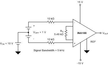 Figure 54. Example Application with G = 10 V/V and a 1-V Differential Voltage
Resistor-adjustable INAs such as the INA188 show the lowest gain error in G = 1 because of the inherently well-matched drift of the internal resistors of the differential amplifier. At gains greater than 1 (for instance, G = 10 V/V or G = 100 V/V) the gain error becomes a significant error source because of the contribution of the resistor drift of the 25-kΩ feedback resistors in conjunction with the external gain resistor. Except for very high-gain applications, gain drift is by far the largest error contributor compared to other drift errors, such as offset drift. The INA188 offers the lowest gain error over temperature in the marketplace for both G > 1 and G = 1 (no external gain resistor). Table 3 summarizes the major error sources in common INA applications and compares the two cases of G = 1 (no external resistor) and G = 10 (5.49-kΩ external resistor). As explained in Table 3, although the static errors (absolute accuracy errors) in G = 1 are almost twice as great as compared to G = 10, there are much fewer drift errors because of the much lower gain error drift. In most applications, these static errors can readily be removed during calibration in production. All calculations refer the error to the input for easy comparison and system evaluation.
Table 3. Error Calculation
| ERROR SOURCE | ERROR CALCULATION | SPECIFICATION | G = 10 ERROR (ppm) | G = 1 ERROR (ppm) |
|---|---|---|---|---|
| ABSOLUTE ACCURACY AT 25°C | ||||
| Input offset voltage | VOSI / VDIFF | 65 μV | 65 | 65 |
| Output offset voltage | VOSO / (G × VDIFF) | 180 μV | 18 | 180 |
| Input offset current | IOS × maximum (RS+, RS–) / VDIFF | 5 nA | 50 | 50 |
| Common-mode rejection ratio | VCM / (10CMRR/20 × VDIFF) | 104 dB (G = 10), 84 dB (G = 1) |
20 | 501 |
| Total absolute accuracy error (ppm) | 153 | 796 | ||
| DRIFT TO 105°C | ||||
| Gain drift | GTC × (TA – 25) | 35 ppm/°C (G = 10), 1 ppm/°C (G = 1) |
2800 | 80 |
| Input offset voltage drift | (VOSI_TC / VDIFF) × (TA – 25) | 0.15 μV/°C | 12 | 12 |
| Output offset voltage drift | [VOSO_TC / ( G × VDIFF)] × (TA – 25) | 0.85 μV/°C | 6.8 | 68 |
| Offset current drift | IOS_TC × maximum (RS+, RS–) × (TA – 25) / VDIFF |
60 pA/°C | 48 | 48 |
| Total drift error (ppm) | 2867 | 208 | ||
| RESOLUTION | ||||
| Gain nonlinearity | 5 ppm of FS | 5 | 5 | |
| Voltage noise (1 kHz) |  |
eNI = 18, eNO = 110 |
9 | 47 |
| Total resolution error (ppm) | 14 | 52 | ||
| TOTAL ERROR | ||||
| Total error (ppm) | Total error = sum of all error sources | 3034 | 1056 | |