ZHCSMV7B February 2020 – May 2021 ISO1640 , ISO1641
PRODUCTION DATA
- 1 特性
- 2 应用
- 3 说明
- 4 Revision History
- 5 Pin Configuration and Functions
-
6 Specifications
- 6.1 Absolute Maximum Ratings
- 6.2 ESD Ratings
- 6.3 Recommended Operating Conditions
- 6.4 Thermal Information
- 6.5 Power Ratings
- 6.6 Insulation Specifications
- 6.7 Safety-Related Certifications
- 6.8 Safety Limiting Values
- 6.9 Electrical Characteristics
- 6.10 Supply Current Characteristics
- 6.11 Timing Requirements
- 6.12 I2C Switching Characteristics
- 6.13 GPIO Switching Characteristics
- 6.14 Insulation Characteristics Curves
- 6.15 Typical Characteristics
- 7 Parameter Measurement Information
- 8 Detailed Description
- 9 Application and Implementation
- 10Power Supply Recommendations
- 11Layout
- 12Device and Documentation Support
- 13Mechanical, Packaging, and Orderable Information
封装选项
机械数据 (封装 | 引脚)
散热焊盘机械数据 (封装 | 引脚)
- DW|16
订购信息
9.1.1 I2C Bus Overview
The inter-integrated circuit (I2C) bus is a single-ended, multi-master, 2-wire bus for efficient inter-IC communication in half-duplex mode.
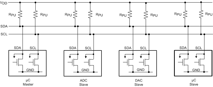
I2C uses open-drain technology, requiring two lines, serial data (SDA) and serial clock (SCL), to be connected to VDD by resistors (see Figure 9-1). Pulling the line to ground is considered a logic zero while letting the line float is a logic one. This logic is used as a channel access method. Transitions of logic states must occur while the SCL pin is low. Transitions while the SCL pin is high indicate START and STOP conditions. Typical supply voltages are 3.3 V and 5 V, although systems with higher or lower voltages are allowed.
 Figure 9-1 I2C Bus
I2C communication uses a 7-bit address space with 16 reserved addresses, so a theoretical maximum of 112 nodes can communicate on the same bus. In practice, however, the number of nodes is limited by the specified, total bus capacitance of 400 pF, which also restricts communication distances to a few meters.
The specified signaling rates for the ISO164x devices are 100 kbps (standard mode), 400 kbps (fast mode), 1.7 Mbps (fast mode plus).
The bus has two roles for nodes: master and slave. A master node issues the clock and slave addresses, and also initiates and ends data transactions. A slave node receives the clock and addresses and responds to requests from the master. Figure 9-2 shows a typical data transfer between master and slave.
 Figure 9-2 Timing Diagram of a Complete Data Transfer
The master initiates a transaction by creating a START condition, following by the 7-bit address of the slave it wishes to communicate with. This is followed by a single read and write (R/W) bit, representing whether the master wishes to write to (0), or to read from (1) the slave. The master then releases the SDA line to allow the slave to acknowledge the receipt of data.
The slave responds with an acknowledge bit (ACK) by pulling the SDA pin low during the entire high time of the 9th clock pulse on the SCL signal, after which the master continues in either transmit or receive mode (according to the R/W bit sent), while the slave continues in the complementary mode (receive or transmit, respectively).
The address and the 8-bit data bytes are sent most significant bit (MSB) first. The START bit is indicated by a high-to-low transition of SDA while SCL is high. The STOP condition is created by a low-to-high transition of SDA while SCL is high.
If the master writes to a slave, it repeatedly sends a byte with the slave sending an ACK bit. In this case, the master is in master-transmit mode and the slave is in slave-receive mode.
If the master reads from a slave, it repeatedly receives a byte from the slave, while acknowledging (ACK) the receipt of every byte but the last one (see Figure 9-3). In this situation, the master is in master-receive mode and the slave is in slave-transmit mode.
The master ends the transmission with a STOP bit, or may send another START bit to maintain bus control for further transfers.
 Figure 9-3 Transmit or Receive Mode Changes During a Data Transfer
When writing to a slave, a master mainly operates in transmit-mode and only changes to receive-mode when receiving acknowledgment from the slave.
When reading from a slave, the master starts in transmit-mode and then changes to receive-mode after sending a READ request (R/W bit = 1) to the slave. The slave continues in the complementary mode until the end of a transaction.
The master ends a reading sequence by not acknowledging (NACK) the last byte received. This procedure resets the slave state machine and allows the master to send the STOP command.